IR MOSFET
StrongIRFET™
IRF60R217
Application
Brushed Motor drive applications
BLDC Motor drive applications
Battery powered circuits
Half-bridge and full-bridge topologies
Synchronous rectifier applications
Resonant mode power supplies
OR-ing and redundant power switches
DC/DC and AC/DC converters
DC/AC Inverters
Benefits
Improved Gate, Avalanche and Dynamic dV/dt Ruggedness
Fully Characterized Capacitance and Avalanche SOA
Enhanced body diode dV/dt and dI/dt Capability
Lead-Free, RoHS Compliant
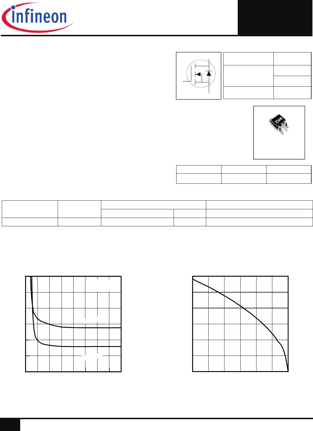
Fig 1. Typical On-Resistance vs. Gate Voltage
Fig 2. Maximum Drain Current vs. Case Temperature
G D S
Gate Drain Source
D-Pak
IRF60R217
D
G
S
Base part number Package Type Standard Pack Orderable Part Number
Form Quantity
IRF60R217 D-Pak
Tape and Reel 2000 IRF60R217
1
2016-01-05
D
S
G
V
DSS
60V
R
DS(on)
typ.
8.0m
max
9.9m
I
D
58A
25 50 75 100 125 150 175
T
C
, Case Temperature (°C)
0
10
20
30
40
50
60
I
D
,
D
r
a
i
n
C
u
r
r
e
n
t
(
A
)
4 6 8 10 12 14 16 18 20
V
GS,
Gate -to -Source Voltage (V)
0
5
10
15
20
25
30
R
D
S
(
o
n
)
,
D
r
a
i
n
-
t
o
-
S
o
u
r
c
e
O
n
R
e
s
i
s
t
a
n
c
e
(
m
)
I
D
= 35A
T
J
= 25°C
T
J
= 125°C
IRF60R217
2
2016-01-05
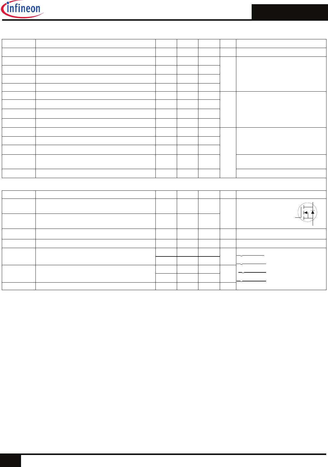
Absolute Maximum Rating
Symbol Parameter Max. Units
A
I
D
@ T
C
= 25°C Continuous Drain Current, V
GS
@ 10V (Silicon Limited) 58
I
D
@ T
C
= 100°C Continuous Drain Current, V
GS
@ 10V (Silicon Limited) 41
I
DM
Pulsed Drain Current  217
P
D
@T
C
= 25°C Maximum Power Dissipation 83 W
Linear Derating Factor 0.56 W/°C
V
GS
Gate-to-Source Voltage ± 20 V
T
J
T
STG
Operating Junction and
Storage Temperature Range
-55 to + 175
°C
Soldering Temperature, for 10 seconds (1.6mm from case) 300
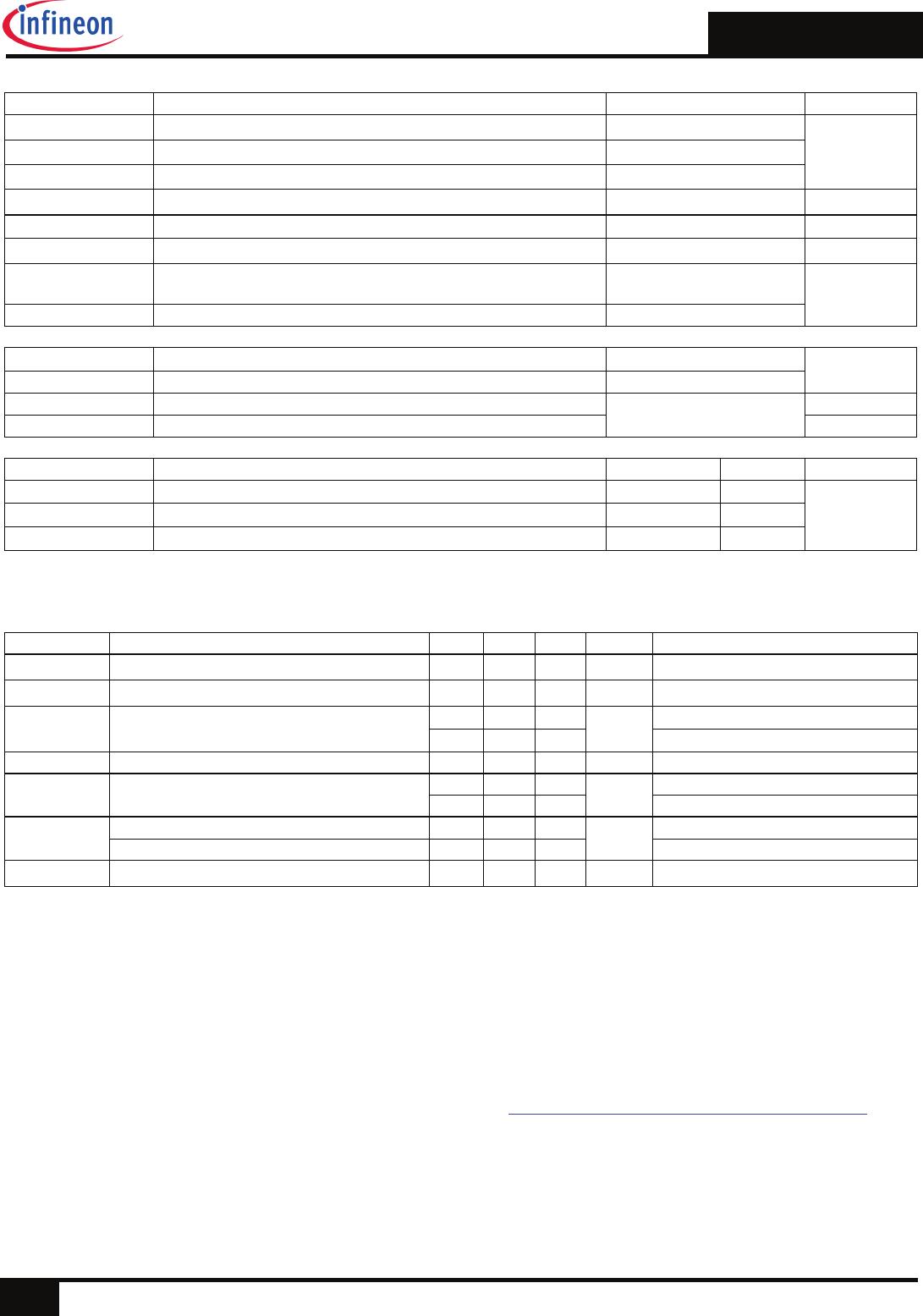
Avalanche Characteristics
E
AS (Thermally limited)
Single Pulse Avalanche Energy 
85
mJ
E
AS (Thermally limited)
Single Pulse Avalanche Energy 
124
I
AR
Avalanche Current
See Fig 15, 16, 23a, 23b
A
E
AR
Repetitive Avalanche Energy mJ
Thermal Resistance
Symbol Parameter Typ. Max. Units
R
JC
Junction-to-Case 
––– 1.8
°C/W
R
JA
Junction-to-Ambient (PCB Mount)
––– 50
R
JA
Junction-to-Ambient
––– 110
Static @ T
J
= 25°C (unless otherwise specified)
Symbol Parameter Min. Typ. Max. Units Conditions
V
(BR)DSS
Drain-to-Source Breakdown Voltage 60 ––– ––– V V
GS
= 0V, I
D
= 250µA
V
(BR)DSS
/T
J
Breakdown Voltage Temp. Coefficient ––– 0.047 ––– V/°C Reference to 25°C, I
D
= 1mA
R
DS(on)
Static Drain-to-Source On-Resistance
––– 8.0 9.9 V
GS
= 10V, I
D
= 35A
––– 10 ––– V
GS
= 6.0V, I
D
= 18A
V
GS(th)
Gate Threshold Voltage 2.1 ––– 3.7 V V
DS
= V
GS
, I
D
= 50µA
I
DSS
Drain-to-Source Leakage Current
––– ––– 1.0
µA
V
DS
= 60V, V
GS
= 0V
––– ––– 150 V
DS
= 60V,V
GS
= 0V,T
J
=125°C
I
GSS
Gate-to-Source Forward Leakage ––– ––– 100
nA
V
GS
= 20V
Gate-to-Source Reverse Leakage ––– ––– -100 V
GS
= -20V
R
G
Gate Resistance ––– 2.0 –––

m
Notes:
 Repetitive rating; pulse width limited by max. junction temperature.
Limited by T
Jmax
, starting T
J
= 25°C, L = 0.14mH, R
G
= 50, I
AS
= 35A, V
GS
=10V.
 I
SD
35A, di/dt 862A/µs, V
DD
V
(BR)DSS
, T
J
175°C.
 Pulse width 400µs; duty cycle 2%.
C
oss
eff. (TR) is a fixed capacitance that gives the same charging time as C
oss
while V
DS
is rising from 0 to 80% V
DSS
.
C
oss
eff. (ER) is a fixed capacitance that gives the same energy as C
oss
while V
DS
is rising from 0 to 80% V
DSS
.
R
is measured at T
J
approximately 90°C.
When mounted on 1" square PCB (FR-4 or G-10 Material). For recommended footprint and soldering techniques refer to
application note #AN-994.please refer to application note to AN-994: http://www.irf.com/technical-info/appnotes/an-994.pdf
Limited by T
Jmax
, starting T
J
= 25°C, L = 1mH, R
G
= 50, I
AS
= 16A, V
GS
=10V.
IRF60R217
3
2016-01-05
Dynamic Electrical Characteristics @ T
J
= 25°C (unless otherwise specified)
Symbol Parameter Min. Typ. Max. Units Conditions
gfs Forward Transconductance 120 ––– ––– S V
DS
= 10V, I
D
= 35A
Q
g
Total Gate Charge ––– 40 66
I
D
= 35A
Q
gs
Gate-to-Source Charge ––– 10 ––– V
DS
= 30V
Q
gd
Gate-to-Drain Charge ––– 12 ––– V
GS
= 10V
Q
sync
Total Gate Charge Sync. (Qg– Qgd) ––– 28 –––
t
d(on)
Turn-On Delay Time ––– 7.6 –––
ns
V
DD
=30V
t
r
Rise Time ––– 29 ––– I
D
= 35A
t
d(off)
Turn-Off Delay Time ––– 21 –––
R
G
= 2.7
t
f
Fall Time ––– 12 –––
V
GS
= 10V
C
iss
Input Capacitance ––– 2170 –––
pF
V
GS
= 0V
C
oss
Output Capacitance ––– 210 ––– V
DS
= 25V
C
rss
Reverse Transfer Capacitance ––– 130 –––
ƒ = 1.0MHz, See Fig. 7
C
oss eff.(ER)
Effective Output Capacitance
(Energy Related)
––– 228 ––– V
GS
= 0V, VDS = 0V to 48V
C
oss eff.(TR)
Output Capacitance (Time Related) ––– 283 ––– V
GS
= 0V, VDS = 0V to 48V
Diode Characteristics
Symbol Parameter Min. Typ. Max. Units Conditions
I
S
Continuous Source Current
––– ––– 58
A
MOSFET symbol
(Body Diode)
showing the
I
SM
Pulsed Source Current
––– ––– 217
integral reverse
(Body Diode) p-n junction diode.
V
SD
Diode Forward Voltage ––– ––– 1.2 V T
J
= 25°C,I
S
= 35A,V
GS
= 0V 
dv/dt Peak Diode Recovery dv/dt  ––– 18 ––– V/ns T
J
= 175°C,I
S
= 35A,V
DS
= 60V
t
rr
Reverse Recovery Time
––– 27 –––
ns
T
J
= 25°C V
DD
= 51V
––– 30 ––– T
J
= 125°C I
F
= 35A,
Q
rr
Reverse Recovery Charge
––– 26 –––
nC
T
J
= 25°C di/dt = 100A/µs 
––– 33 ––– T
J
= 125°C
I
RRM
Reverse Recovery Current ––– 1.7 ––– A
T
J
= 25°C
nC
D
S
G

IRF60R217

Mfr. #:
Manufacturer:
Infineon / IR
Description:
MOSFET 60V, 58A, 9.9 mOhm 40 nC Qg
Lifecycle:
New from this manufacturer.
Delivery:
DHL FedEx Ups TNT EMS
Payment:
T/T Paypal Visa MoneyGram Western Union

Products related to this Datasheet