IRF60R217
4
2016-01-05
Fig 6. Normalized On-Resistance vs. Temperature
Fig 5. Typical Transfer Characteristics
Fig 4. Typical Output Characteristics
Fig 3. Typical Output Characteristics
Fig 7. Typical Capacitance vs. Drain-to-Source Voltage
Fig 8. Typical Gate Charge vs. Drain-to-Source Voltage
0.1 1 10 100
V
DS
, Drain-to-Source Voltage (V)
100
1000
10000
C
,
C
a
p
a
c
i
t
a
n
c
e
(
p
F
)
V
GS
= 0V, f = 1 MHZ
C
iss
= C
gs
+ C
gd
, C
ds
SHORTED
C
rss
= C
gd
C
oss
= C
ds
+ C
gd
C
oss
C
rss
C
iss
-60 -40 -20 0 20 40 60 80 100120140160180
T
J
, Junction Temperature (°C)
0.5
1.0
1.5
2.0
2.5
R
D
S
(
o
n
)
,
D
r
a
i
n
-
t
o
-
S
o
u
r
c
e
O
n
R
e
s
i
s
t
a
n
c
e
(
N
o
r
m
a
l
i
z
e
d
)
I
D
= 35A
V
GS
= 10V
0 102030405060
Q
G
,
Total Gate Charge (nC)
0
2
4
6
8
10
12
14
V
G
S
,
G
a
t
e
-
t
o
-
S
o
u
r
c
e
V
o
l
t
a
g
e
(
V
)
V
DS
= 48V
V
DS
= 30V
VDS= 12V
I
D
= 35A
0.1 1 10 100
V
DS
, Drain-to-Source Voltage (V)
1
10
100
1000
I
D
,
D
r
a
i
n
-
t
o
-
S
o
u
r
c
e
C
u
r
r
e
n
t
(
A
)
VGS
TOP 15V
10V
8.0V
7.0V
6.0V
5.5V
5.0V
BOTTOM 4.5V
60µs
PULSE WI DTH
Tj = 25°C
4.5V
0.1 1 10 100
V
DS
, Drain-to-Source Voltage (V)
1
10
100
1000
I
D
,
D
r
a
i
n
-
t
o
-
S
o
u
r
c
e
C
u
r
r
e
n
t
(
A
)
4.5V
60µs
PULSE WIDTH
Tj = 175°C
VGS
TOP 15V
10V
8.0V
7.0V
6.0V
5.5V
5.0V
BOTTOM 4.5V
2 3 4 5 6 7 8
V
GS
, Gate-to-Source Voltage (V)
0.1
1
10
100
1000
I
D
,
D
r
a
i
n
-
t
o
-
S
o
u
r
c
e
C
u
r
r
e
n
t
(
A
)
T
J
= 25°C
T
J
= 175°C
V
DS
= 25V
60µs PULSE WIDTH
IRF60R217
5
2016-01-05
Fig 10. Maximum Safe Operating Area
Fig 11. Drain-to-Source Breakdown Voltage
Fig 9. Typical Source-Drain Diode Forward Voltage
Fig 13. Typical On-Resistance vs. Drain Current
0.2 0.4 0.6 0.8 1.0 1.2 1.4 1.6
V
SD
, Source-to-Drain Voltage (V)
0.1
1
10
100
1000
I
S
D
,
R
e
v
e
r
s
e
D
r
a
i
n
C
u
r
r
e
n
t
(
A
)
T
J
= 25°C
T
J
= 175°C
V
GS
= 0V
-60 -40 -20 0 20 40 60 80 100120140160180
T
J
, Temperature ( °C )
60
65
70
75
V
(
B
R
)
D
S
S
,
D
r
a
i
n
-
t
o
-
S
o
u
r
c
e
B
r
e
a
k
d
o
w
n
V
o
l
t
a
g
e
(
V
)
Id = 1.0mA
0 102030405060
V
DS,
Drain-to-Source Voltage (V)
0.0
0.1
0.1
0.2
0.2
0.3
0.3
0.4
E
n
e
r
g
y
(
µ
J
)
Fig 12. Typical C
oss
Stored Energy
0 20 40 60 80 100 120 140 160
I
D
, Drain Current (A)
4
8
12
16
20
24
R
D
S
(
o
n
)
,
D
r
a
i
n
-
t
o
-
S
o
u
r
c
e
O
n
R
e
s
i
s
t
a
n
c
e
(
m
)
VGS = 6.0V
VGS = 7.0V
VGS = 8.0V
VGS = 10V
0.1 1 10 100
V
DS
, Drain-toSource Voltage (V)
0.01
0.1
1
10
100
1000
I
D
,
D
r
a
i
n
-
t
o
-
S
o
u
r
c
e
C
u
r
r
e
n
t
(
A
)
Tc = 25°C
Tj = 175°C
Single Pulse
1msec
10msec
OPERATION IN THIS AREA
LIMITED BY RDS(on)
100µsec
DC
IRF60R217
6
2016-01-05
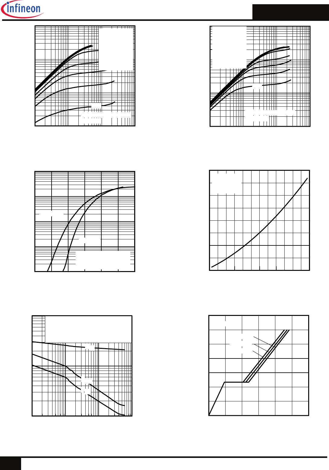
Fig 14. Maximum Effective Transient Thermal Impedance, Junction-to-Case
Fig 16. Maximum Avalanche Energy vs. Temperature
Fig 15. Avalanche Current vs. Pulse Width
Notes on Repetitive Avalanche Curves, Figures 15, 16:
(For further info, see AN-1005 at www.irf.com)
1.Avalanche failures assumption:
Purely a thermal phenomenon and failure occurs at a
temperature far in excess of T
jmax
. This is validated for every
part type.
2. Safe operation in Avalanche is allowed as long asT
jmax
is not
exceeded.
3. Equation below based on circuit and waveforms shown in Figures
23a, 23b.
4. P
D (ave)
= Average power dissipation per single avalanche pulse.
5. BV = Rated breakdown voltage (1.3 factor accounts for voltage
increase during avalanche).
6. I
av
= Allowable avalanche current.
7. T = Allowable rise in junction temperature, not to exceed T
jmax
(assumed as 25°C in Figures 14, 15).
t
av
= Average time in avalanche.
D = Duty cycle in avalanche = tav ·f
Z
thJC
(D, t
av
) = Transient thermal resistance, see Figure 14)
PD (ave) = 1/2 ( 1.3·BV·I
av
) = T/ Z
thJC
I
av
= 2T/ [1.3·BV·Z
th
]
E
AS (AR)
= P
D (ave)·
t
av

1E-006 1E-005 0.0001 0.001 0.01 0.1
t
1
, Rectangular Pulse Duration (sec)
0.001
0.01
0.1
1
10
T
h
e
r
ma
l
R
e
s
p
o
n
s
e
(
Z
t
h
J
C
)
°
C
/
W
0.20
0.10
D = 0.50
0.02
0.01
0.05
SINGLE PULSE
( THERMAL RESPONSE )
Notes:
1. Duty Factor D = t1/t2
2. Peak Tj = P dm x Zthjc + Tc
25 50 75 100 125 150 175
Starting T
J
, Junction Temperature (°C)
0
20
40
60
80
100
E
A
R
,
A
v
a
l
a
n
c
h
e
E
n
e
r
g
y
(
m
J
)
TOP Single Pulse
BOTTOM 1.0% Duty Cycle
I
D
= 35A
1.0E-06 1.0E-05 1.0E-04 1.0E-03 1.0E-02 1.0E-01
tav (sec)
0.1
1
10
100
A
v
a
l
a
n
c
h
e
C
u
r
r
e
n
t
(
A
)
Allowed avalanche Current vs avalanche
pulsewidth, tav, assuming

j = 25°C and
Tstart = 150°C.
Allowed avalanche Current vs avalanche
pulsewidth, tav, assuming
Tj = 150°C and
Tstart = 25°C (Single Pulse)

IRF60R217

Mfr. #:
Manufacturer:
Infineon / IR
Description:
MOSFET 60V, 58A, 9.9 mOhm 40 nC Qg
Lifecycle:
New from this manufacturer.
Delivery:
DHL FedEx Ups TNT EMS
Payment:
T/T Paypal Visa MoneyGram Western Union

Products related to this Datasheet