A.2 Module PCB Footprint
Dimensions in mm
Note: All modules have the same footprint.
Figure 8 Module PCB footprint
RF note for –M00 modules with ceramic antenna: No components, ground plane or tracks on any layer of
the mother board should be placed within 20mm of the 3 free sides of the antenna. Tracks etc may be placed
adjacent to the can, but should not extend past the can towards the antenna end of the module for 20mm
from the antenna.
16 JN-DS-JN5139-xxx-Myy 1v6 © NXP Laboratories UK 2010
A.3 Ordering Information
Ordering Code Format:
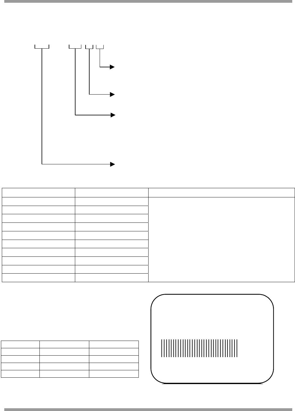
JN5139 - XXX - M / Y1Y2 Y3 Y4
Shipping
T Tape Mounted 500-piece reel (00, 03, 04 modules only)
VTa
p
e Mounted 200-
p
iece reel
(
01
,
02 modules onl
y)
Temp Range / Device Status
R1 -20°C to +70°C
Module Type
00 Standard Power, Ceramic antenna
01 Standard Power, SMA connector
02 High Power, SMA connector
03 Standard Power, uFl connector – use for new designs
04 High power, uFl connector– use for new designs
Software Variant
001 IEEE802.15.4 Stack
Z01 ZigBee Stack
Part Number Ordering Code Description
JN5139-001-M00R1T JN5139-001-M/00R1T
JN5139 module, variant as detailed above
JN5139-001-M01R1V JN5139-001-M/01R1V
JN5139-001-M02R1V JN5139-001-M/02R1V
JN5139-001-M03R1T JN5139-001-M/03R1T
JN5139-001-M04R1T JN5139-001-M/04R1T
JN5139-Z01-M00R1T JN5139-Z01-M/00R1T
JN5139-Z01-M01R1V JN5139-Z01-M/01R1V
JN5139-Z01-M02R1V JN5139-Z01-M/02R1V
JN5139-Z01-M03R1T JN5139-Z01-M/03R1T
JN5139-Z01-M04R1T JN5139-Z01-M/04R1T
Label line 1: IC ID Number
Label line 2: FCC ID Number
Label line 3: Part Number
Label line 4: Barcode Label
Label line 5: YYWWTNNNNN (see below)
Identifier Description Format
YY Year 06 (example)
WW Week 45 (example)
T Module type
NNNNN Serial Number
IC: 7438A-CYO5139M0
FCC ID: TYOJN5139M0
JN5139 -XXX-
MY
1
Y
2
Y
3
YYWWTNNNNN
Figure 9: Example module labelling for FCC approved modules
© NXP Laboratories UK 2010 JN-DS-JN5139-xxx-Myy 1v6 17
A.4 Tape and Reel Information:
A.4.1 Tape Orientation and dimensions
All dimensions are in mm
Module type: A B W F E P0 P1 P2 T Cover Tape
width (W)
JN5139-xxx-M00/03 18.4 30.4 44 20.2 1.75 4.0 2.0 24.0 3.4 37.5
JN5139-xxx-M01 18.4 30.4 56 26.2 1.75 4.0 2.0 24.0 11.2 49.5
JN5139-xxx-M02 18.5 41.5 56 26.2 1.75 4.0 2.0 24.0 11.1 49.5
JN5139-xxx-M04 18.5 40.9 56 26.2 1.75 4.0 2.0 24.0 3.4 49.5
Tolerance ±0.1 ±0.1 ±0.3 ±0.1 +0.1 ±0.1 ±0.1 ±0.1 ±0.1 ±0.1
A.4.2 Cover tape details
Thickness (T) 0.061mm
4
Surface resistivity (component side) 10 to 10
7
Ohms/sq
Surface resistivity (component side) Non-conductive
Backing type: Polyester
Adhesive type: PSA
Sealing: Room ambient
18 JN-DS-JN5139-xxx-Myy 1v6 © NXP Laboratories UK 2010

JN5139-Z01-M/01R1V

Mfr. #:
Manufacturer:
NXP Semiconductors
Description:
Zigbee Modules (802.15.4) WIRELESS MCU ZIGBEE
Lifecycle:
New from this manufacturer.
Delivery:
DHL FedEx Ups TNT EMS
Payment:
T/T Paypal Visa MoneyGram Western Union