©1988 Fairchild Semiconductor Corporation www.fairchildsemi.com
74AC02, 74ACT02 Rev. 1.5.1 2
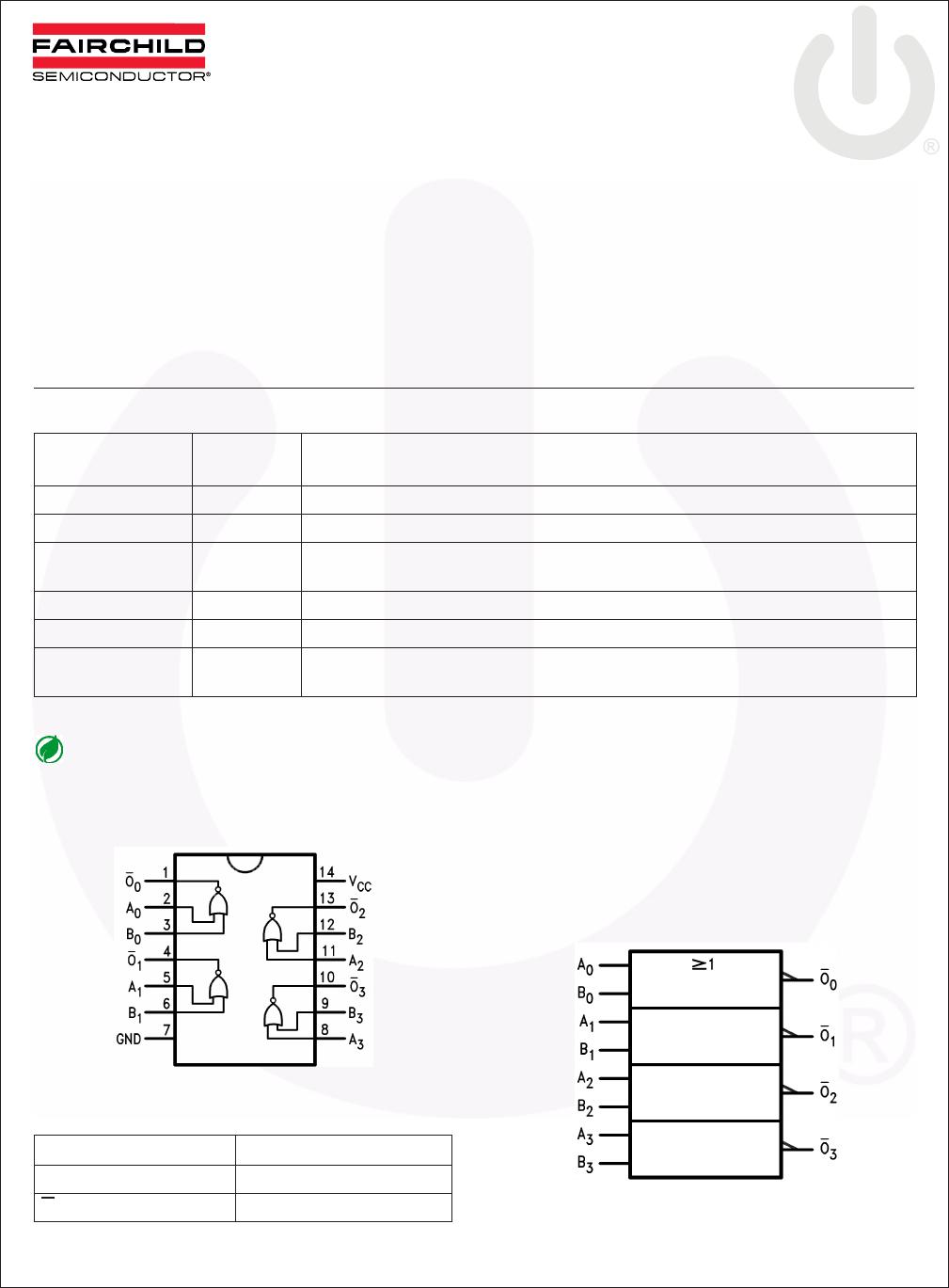
74AC02, 74ACT02 — Quad 2-Input NOR Gate
Absolute Maximum Ratings
Stresses exceeding the absolute maximum ratings may damage the device. The device may not function or be
operable above the recommended operating conditions and stressing the parts to these levels is not recommended.
In addition, extended exposure to stresses above the recommended operating conditions may affect device reliability.
The absolute maximum ratings are stress ratings only.
Recommended Operating Conditions
The Recommended Operating Conditions table defines the conditions for actual device operation. Recommended
operating conditions are specified to ensure optimal performance to the datasheet specifications. Fairchild does not
recommend exceeding them or designing to absolute maximum ratings.
Symbol Parameter Rating
V
CC
Supply Voltage –0.5V to +7.0V
I
IK
DC Input Diode Current
V
I
=
–0.5V
V
I
=
V
CC
+ 0.5V
–20mA
+20mA
V
I
DC Input Voltage –0.5V to V
CC
+ 0.5V
I
OK
DC Output Diode Current
V
O
=
–0.5V
V
O
=
V
CC
+ 0.5V
–20mA
+20mA
V
O
DC Output Voltage –0.5V to V
CC
+ 0.5V
I
O
DC Output Source or Sink Current ±50mA
I
CC
or I
GND
DC V
CC
or Ground Current per Output Pin ±50mA
T
STG
Storage Temperature –65°C to +150°C
T
J
Junction Temperature 140°C
Symbol Parameter Rating
V
CC
Supply Voltage
AC
ACT
2.0V to 6.0V
4.5V to 5.5V
V
I
Input Voltage 0V to V
CC
V
O
Output Voltage 0V to V
CC
T
A
Operating Temperature –40°C to +85°C
∆
V
/
∆
t Minimum Input Edge Rate, AC Devices:
V
IN
from 30% to 70% of V
CC
,
V
CC
@ 3.3V, 4.5V, 5.5V
125mV/ns
∆
V
/
∆
t Minimum Input Edge Rate, ACT Devices:
V
IN
from 0.8V to 2.0V, V
CC
@ 4.5V, 5.5V
125mV/ns