OP400 Data Sheet
Rev. H | Page 2 of 16
TABLE OF CONTENTS
Features .............................................................................................. 1
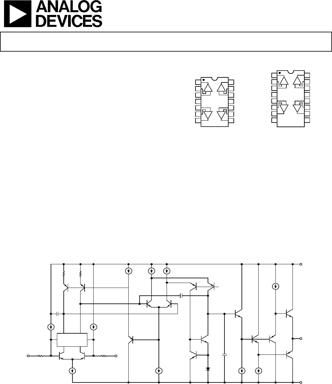
Functional Block Diagrams ............................................................. 1
General Description ......................................................................... 1
Revision History ............................................................................... 2
Specifications ..................................................................................... 3
Electrical Characteristics ............................................................. 3
Absolute Maximum Ratings ............................................................ 5
Thermal Resistance ...................................................................... 5
ESD Caution .................................................................................. 5
Typical Performance Characteristics ..............................................6
Applications ..................................................................................... 11
Dual Low Power Instrumentation Amplifier ......................... 11
Bipolar Current Transmitter ..................................................... 12
Differential Output Instrumentation Amplifier .................... 12
Multiple Output Tracking Voltage Reference ......................... 13
Outline Dimensions ....................................................................... 14
Ordering Guide .......................................................................... 15
SMD Parts and Equivalents ...................................................... 15
REVISION HISTORY
1/13—Rev. G to Rev. H
Changes to Features Section and General Description Section ........ 1
Changes to Ordering Guide ........................................................... 15
2/11—Rev. F to Rev. G
Added S Package to Storage Temperature Range in Table 4 ....... 5
Updated Outline Dimensions ....................................................... 15
12/08—Rev. E to Rev. F
Added New Figure 28, Renumbered Sequentially ..................... 10
Updated Outline Dimensions ....................................................... 15
1/07—Rev. D to Rev. E
Updated Format .................................................................. Universal
Changes to Figure 1 and Figure 2 ................................................... 1
Removed Figure 4 ............................................................................. 4
Changes to Table 3 ............................................................................ 4
Changes to Figure 16 through Figure 19, Figure 21 .................... 8
Changes to Figure 27 ........................................................................ 9
Changes to Figure 28 ...................................................................... 10
Changes to Figure 33 ...................................................................... 13
Updated Outline Dimensions ....................................................... 14
3/06—Rev. C to Rev. D
Updated Format .................................................................. Universal
Deleted Wafer Test Limits Table ..................................................... 4
New Package Drawing: R-14 ......................................................... 15
Updated Outline Dimensions ....................................................... 15
Changes to Ordering Guide .......................................................... 16
6/03—Rev. B to Rev. C
Edits to Specifications ....................................................................... 2
10/02—Rev. A to Rev. B
Addition of Absolute Maximum Ratings ....................................... 5
Edits to Outline Dimensions......................................................... 12
4/02—Rev. 0 to Rev. A
Edits to Features................................................................................. 1
Edits to Ordering Information ........................................................ 1
Edits to Pin Connections .................................................................. 1
Edits to General Descriptions ..................................................... 1, 2
Edits to Package Type ....................................................................... 2