Data Sheet OP400
Rev. H | Page 11 of 16
APPLICATIONS
The OP400 is inherently stable at all gains and is capable of
driving large capacitive loads without oscillating. Nonetheless,
good supply decoupling is highly recommended. Proper supply
decoupling reduces problems caused by supply line noise and
improves the capacitive load-driving capability of the OP400.
Total supply current can be reduced by connecting the inputs of
an unused amplifier to V−. This turns the amplifier off,
lowering the total supply current.
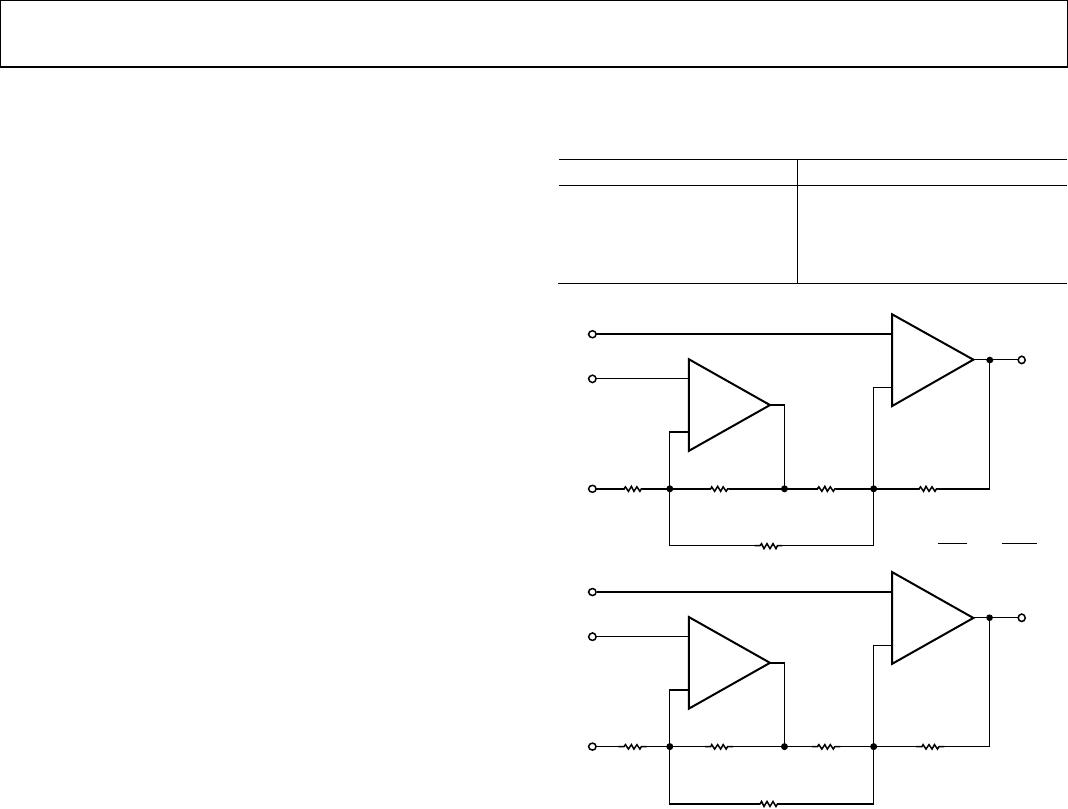
DUAL LOW POWER INSTRUMENTATION
AMPLIFIER
A dual instrumentation amplifier that consumes less than
33 mW of power per channel is shown in Figure 31. The linear-
ity of the instrumentation amplifier exceeds 16 bits in gains of 5 to
200 and is better than 14 bits in gains from 200 to 1000. CMRR
is above 115 dB (G = 1000). Offset voltage drift is typically
0.4 μV/°C over the military temperature range, which is
comparable to the best monolithic instrumentation amplifiers.
The bandwidth of the low power instrumentation amplifier is
a function of gain and is shown in Table 6.
The output signal is specified with respect to the reference
input, which is normally connected to analog ground. The
reference input can be used to offset the output from −10 V to
+10 V if required.
Table 6. Gain Bandwidth
Gain Bandwidth
5 150 kHz
100 7.5 kHz
1000 500 Hz
–
+
20kΩ5kΩ5kΩ
20kΩ
REFERENCE
V
IN
V
IN
R
G
R
G
V
OUT
V
OUT
–
+
20kΩ5kΩ5kΩ
20kΩ
REFERENCE
V
IN
R
G
V
OUT
40,000
= 5 +
00304-030
1/4
OP400A
+
–
1/4
OP400A
+
–
1/4
OP400A
+
–
1/4
OP400A
+
–
Figure 31. Dual Low Power Instrumentation Amplifier

