REV. B
AD9883A
–21–
13 7–0 Post-Coast
This register allows the coast signal to be applied follow-
ing the Vsync signal. This is necessary in cases where
post-equalization pulses are present. The step size for this
control is one Hsync period.
The default is 0.
14 7 Hsync Detect
This bit is used to indicate when activity is detected on
the Hsync input pin (Pin 30). If Hsync is held high or
low, activity will not be detected.
Table XXVII. Hsync Detection Results
Detect Function
0No Activity Detected
1Activity Detected
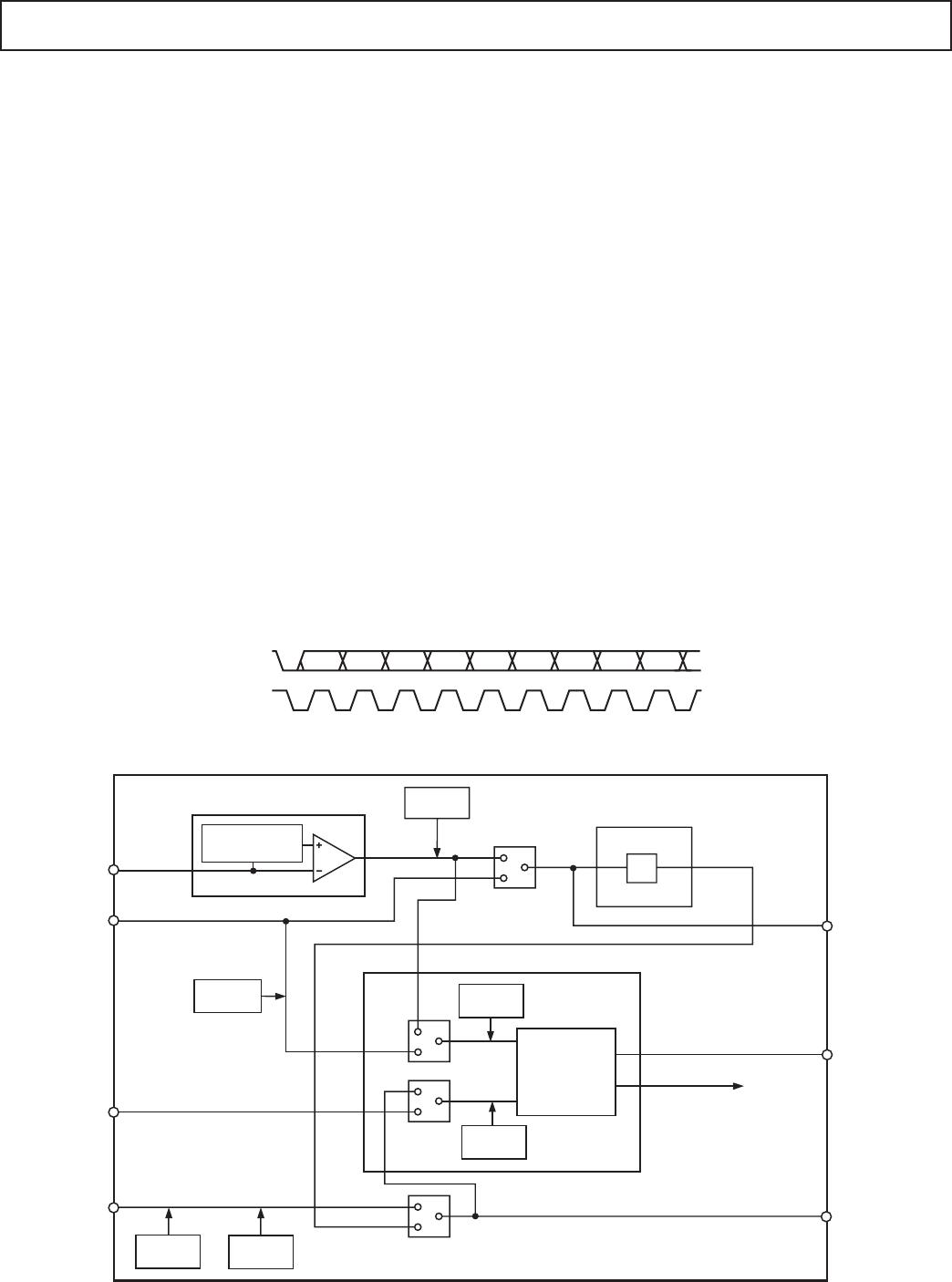
The sync processing block diagram shows where this
function is implemented.
14 6 AHS – Active Hsync
This bit indicates which Hsync input source is being used
by the PLL (Hsync input or Sync-on-Green). Bits 7 and 1
in this register determine which source is used. If both
Hsync and SOG are detected, the user can determine which
has priority via Bit 3 in register 0EH. The user can override
this function via Bit 4 in register 0EH. If the override bit
is set to Logic 1, then this bit will be forced to whatever
the state of Bit 3 in register 0EH is set to.
Table XXVIII. Active Hsync Results
Bit 7 Bit 1 Bit 4,
(Hsync (SOG Reg 0EH
Detect) Detect) (Override) AHS
00 0 Bit 3 in 0EH
01 0 1
10 0 0
11 0 Bit 3 in 0EH
XX 1 Bit 3 in 0EH
AHS = 0 means use the Hsync pin input for Hsync.
AHS = 1 means use the SOG pin input for Hsync.
The override bit is in register 0EH, Bit 4.
14 5 Detected Hsync Input Polarity Status
This bit reports the status of the Hsync input polarity
detection circuit. It can be used to determine the polarity
of the Hsync input. The detection circuit’s location is
shown in the Sync Processing Block Diagram (Figure 12).
Table XXIX. Detected Hsync Input Polarity Status
Hsync Polarity Status Result
0Negative
1 Positive
14 4 Vsync Detect
This bit is used to indicate when activity is detected on
the Vsync input pin (Pin 31). If Vsync is held steady high
or low, activity will not be detected.
Table XXX. Vsync Detection Results
Detect Function
0No Activity Detected
1Activity Detected
The Sync Processing Block Diagram (Figure 12) shows
where this function is implemented.
14 3 AVS – Active Vsync
This bit indicates which Vsync source is being used: the
Vsync input or output from the sync separator. Bit 4 in this
register determines which is active. If both Vsync and
SOG are detected, the user can determine which has
priority via Bit 0 in register 0EH. The user can override this
function via Bit 1 in register 0EH. If the override bit is set
to Logic 1, this bit will be forced to whatever the state of Bit 0
in register 0EH is set.
Table XXXI. Active Vsync Results
AVS = 0 means Vsync input.
AVS = 1 means Sync separator.
The override bit is in register 0EH, Bit 1.
14 2 Detected Vsync Output Polarity Status
This bit reports the status of the Vsync output polarity
detection circuit. It can be used to determine the polarity
of the Vsync output. The detection circuit’s location is-
shown in the Sync Processing Block Diagram (Figure 12).
Table XXXII. Detected Vsync Output Polarity Status
Vsync Polarity Status Result
0Active Low
1Active High
14 1 Sync-on-Green Detect
This bit is used to indicate when sync activity is detected
on the Sync-on-Green input pin (Pin 49).
Table XXXIII. Sync-on-Green Detection Results
Detect Function
0No Activity Detected
1Activity Detected
The Sync Processing Block Diagram (Figure 12) shows
where this function is implemented.
14 0 Detected Coast Polarity Status
This bit reports the status of the Coast input polarity
detection circuit. It can be used to determine the polarity
of the Coast input. The detection circuit’s location is shown
in the Sync Processing Block Diagram (Figure 12).
Bit 4, Reg 14H Bit 1, Reg 0EH
(Vsync Detect) (Override) AVS
100
001
X1Bit 0 in 0EH
REV. B
AD9883A
–22–
Table XXXIV. Detected Coast Input Polarity Status
Polarity Status Result
0Coast Polarity Negative
1Coast Polarity Positive
This indicates that Bit 1 of Register 5 is the 4:2:2 Output
mode select bit.
15 1 4:2:2 Output Mode Select
A bit that configures the output data in 4:2:2 mode.
This mode can be used to reduce the number of data
lines used from 24 down to 16 for applications using
YUV, YCbCr, or YPbPr graphics signals. A timing
diagram for this mode is shown in Figure 9.
Recommended input and output configurations are
shown in Table XXXV.
Table XXXV. 4:2:2 Output Mode Select
Select Output Mode
0 4:2:2
1 4:4:4
Table XXXVI. 4:2:2 Input/Output Configuration
Input
Channel Connection Output Format
Red V U/V
Green Y Y
Blue U High Impedance
2-WIRE SERIAL CONTROL PORT
A 2-wire serial interface control interface is provided. Up to two
AD9883A devices may be connected to the 2-wire serial interface,
with each device having a unique address.
The 2-wire serial interface comprises a clock (SCL) and a bidi-
rectional data (SDA) pin. The analog flat panel interface acts as
a slave for receiving and transmitting data over the serial interface.
When the serial interface is not active, the logic levels on SCL
and SDA are pulled high by external pull-up resistors.
Data received or transmitted on the SDA line must be stable for
the duration of the positive-going SCL pulse. Data on SDA must
change only when SCL is low. If SDA changes state while SCL
is high, the serial interface interprets that action as a start or
stop sequence.
There are five components to serial bus operation:
Start Signal
Slave Address Byte
Base Register Address Byte
Data Byte to Read or Write
Stop Signal
When the serial interface is inactive (SCL and SDA are high)
communications are initiated by sending a start signal. The start
signal is a high-to-low transition on SDA while SCL is high.
This signal alerts all slaved devices that a data transfer sequence
is coming.
The first eight bits of data transferred after a start signal com-
prise a 7-bit slave address (the first seven bits) and a single R/W
Bit (the eighth bit). The R/W Bit indicates the direction of data
transfer, read from (1) or write to (0) the slave device. If the
transmitted slave address matches the address of the device (set by
the state of the SA
1-0
input pins in Table XXXIV, the AD9883A
acknowledges by bringing SDA low on the ninth SCL pulse. If the
addresses do not match, the AD9883A does not acknowledge.
Table XXXVII. Serial Port Addresses
Bit 7 Bit 6 Bit 5 Bit 4 Bit 3 Bit 2 Bit 1
A
6
A
5
A
4
A
3
A
2
A
1
A
0
(MSB)
1001100
1001101
Data Transfer via Serial Interface
For each byte of data read or written, the MSB is the first bit of
the sequence.
If the AD9883A does not acknowledge the master device during
a write sequence, the SDA remains high so the master can gen-
erate a stop signal. If the master device does not acknowledge the
AD9883A during a read sequence, the AD9883A interprets this
as “end of data.” The SDA remains high so the master can
generate a stop signal.
Writing data to specific control registers of the AD9883A requires
that the 8-bit address of the control register of interest be written
after the slave address has been established. This control register
address is the base address for subsequent write operations. The
base address autoincrements by one for each byte of data written
after the data byte intended for the base address. If more bytes
are transferred than there are available addresses, the address will
not increment and remains at its maximum value of 14H. Any base
address higher than 14H will not produce an acknowledge signal.
SDA
SCL
t
BUFF
t
STAH
t
DHO
t
DSU
t
DAL
t
DAH
t
STASU
t
STOSU
Figure 10. Serial Port Read/Write Timing
REV. B
AD9883A
–23–
Data is read from the control registers of the AD9883A in a similar
manner. Reading requires two data transfer operations:
The base address must be written with the R/W Bit of the slave
address byte low to set up a sequential read operation.
Reading (the R/W Bit of the slave address byte high) begins at
the previously established base address. The address of the read
register autoincrements after each byte is transferred.
To terminate a read/write sequence to the AD9883A, a stop
signal must be sent. A stop signal comprises a low-to-high tran-
sition of SDA while SCL is high.
A repeated start signal occurs when the master device driving
the serial interface generates a start signal without first generating
a stop signal to terminate the current communication. This is
used to change the mode of communication (read, write)
between the slave and master without releasing the serial
interface lines.
Serial Interface Read/Write Examples
Write to one control register
Start Signal
Slave Address Byte (R/W Bit = Low)
Base Address Byte
Data Byte to Base Address
Stop Signal
Write to four consecutive control registers
Start Signal
Slave Address Byte (R/W Bit = Low)
Base Address Byte
Data Byte to Base Address
Data Byte to (Base Address + 1)
Data Byte to (Base Address + 2)
Data Byte to (Base Address + 3)
Stop Signal
Read from one control register
Start Signal
Slave Address Byte (R/W Bit = Low)
Base Address Byte
Start Signal
Slave Address Byte (R/W Bit = High)
Data Byte from Base Address
Stop Signal
Read from four consecutive control registers
Start Signal
Slave Address Byte (R/W Bit = Low)
Base Address Byte
Start Signal
Slave Address Byte (R/W Bit = High)
Data Byte from Base Address
Data Byte from (Base Address + 1)
Data Byte from (Base Address + 2)
Data Byte from (Base Address + 3)
Stop Signal
BIT 7
ACKBIT 6 BIT 5 BIT 4 BIT 3 BIT 2 BIT 1 BIT 0SDA
SCL
Figure 11. Serial Interface—Typical Byte Transfer
SYNC STRIPPER
ACTIVITY
DETECT
NEGATIVE PEAK
CLAMP
COMP
SYNC
SOG
HSYNC IN
ACTIVITY
DETECT
MUX 2
HSYNC OUT
PIXEL CLOCK
MUX 1
SYNC SEPARATOR
INTEGRATOR
VSYNC
SOG OUT
HSYNC OUT
VSYNC OUT
MUX 4
VSYNC IN
1/S
PLL
HSYNC
ACTIVITY
DETECT
AD9883A
CLOCK
GENERATOR
POLARITY
DETECT
POLARITY
DETECT
POLARITY
DETECT
MUX 3
COAST
COAST
Figure 12. Sync Processing Block Diagram

AD9883AKSTZ-140

Mfr. #:
Manufacturer:
Analog Devices Inc.
Description:
Display Interface IC 140MHz Analog interface -SGA FPD
Lifecycle:
New from this manufacturer.
Delivery:
DHL FedEx Ups TNT EMS
Payment:
T/T Paypal Visa MoneyGram Western Union