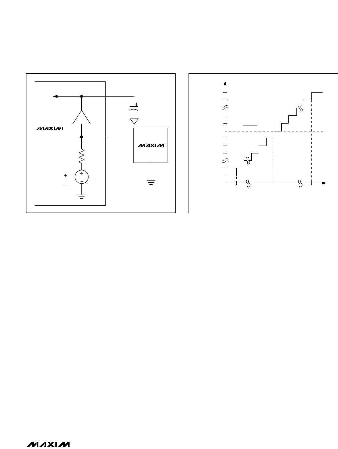
1ppm/°C (max) temperature drift. Connect an external
reference at REFIN as shown in Figure 7. The minimum
impedance is 7kΩ for DC currents in both normal oper-
ation and shutdown. Bypass REFOUT with a 4.7µF low-
ESR capacitor.
Power-On Reset
When power is first applied, the internal power-on-reset
circuitry activates the MAX125/MAX126 with INT =
high, ready to convert. The default conversion mode is
Input Mux A/Single-Channel Conversion. See the
Programming Modes
section if other configurations are
desired.
After the power supplies have been stabilized, the reset
time is 5µs; no conversions should be performed
during this phase. At power-up, data in memory is
undefined.
Software Power-Down
Software power-down is activated by setting bit A3 of
the control word high (Table 1). It is asserted after the
WR or CS rising edge, at which point the ADC immedi-
ately powers down to a low quiescent-current state.
AV
DD
drops to less than 1.5mA, and AV
SS
is reduced
to less than 1mA. The ADC blocks and reference buffer
are turned off, but the digital interface and the refer-
ence remain active for fast power-up recovery. Wake
up the MAX125/MAX126 by writing a control word
(A0–A3, Table 1). The bidirectional interface interprets
a logic zero at A3 as the start signal and powers up in
the mode selected by A0, A1, and A2. The reference
buffer’s settling time and the bypass capacitor’s value
dominate the power-up delay. With the recommended
4.7µF at REFOUT, the power-up delay is typically 5µs.
Transfer Function
The MAX125/MAX126 have bipolar input ranges. Fig-
ure 8 shows the bipolar/output transfer function. Code
transitions occur at successive-integer least significant
bit (LSB) values. Output coding is twos-complement
binary with 1LSB = 610µV for the MAX125 and
1LSB = 305µV for the MAX126.
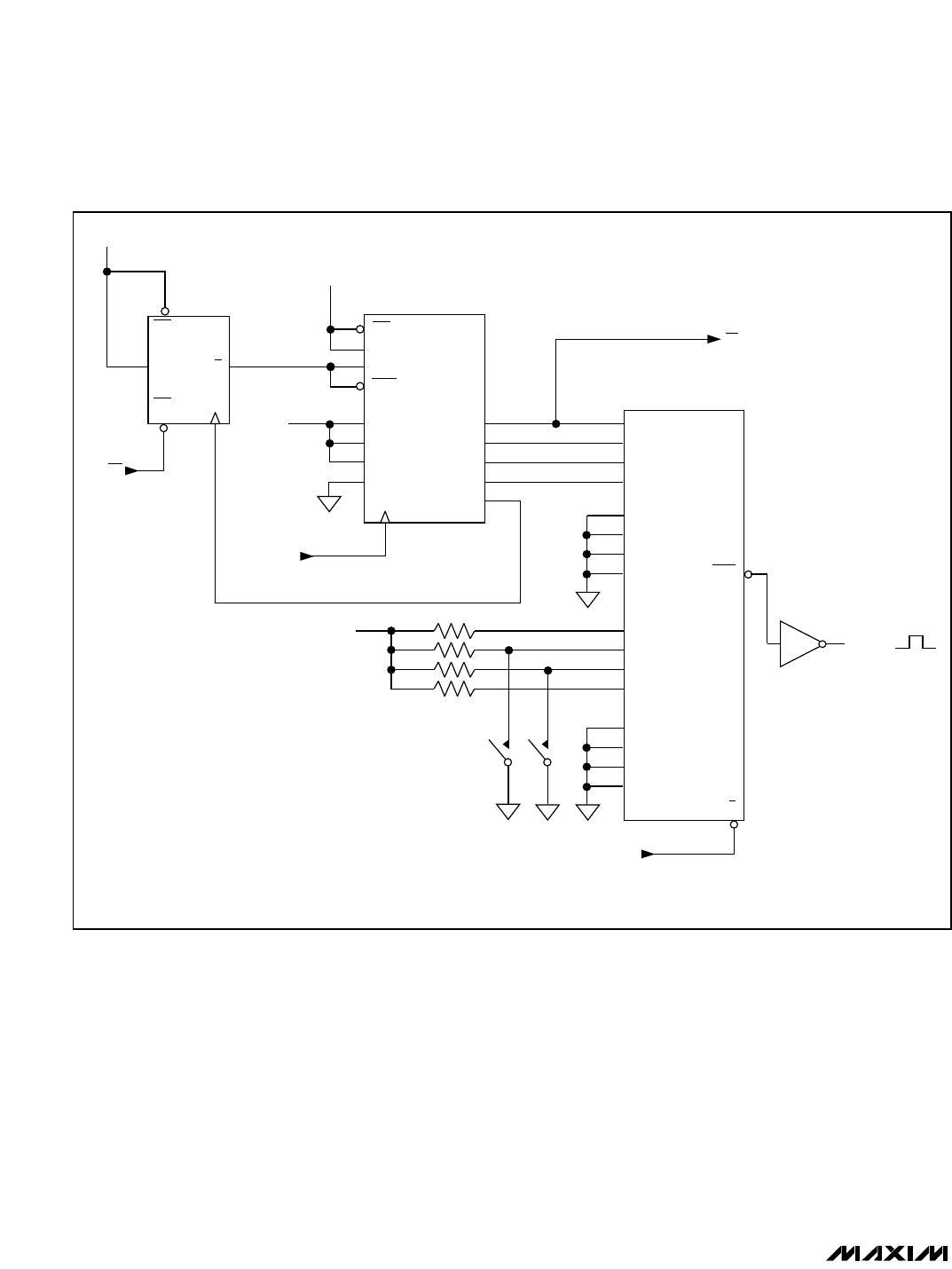
Output Demultiplexer
An output demultiplexer circuit is useful for isolating
data from one channel in a four-channel conversion
sequence. Figure 9’s circuit uses the external 16MHz
clock and the INT signal to generate four RD pulses
and a latch clock to save data from the desired chan-
nel. CS must be low during the four RD pulses. The
channel is selected with the binary coding of two
switches. A 16-bit 16373 latch simplifies layout.
Motor-Control Applications
Vector motor control requires monitoring of the individ-
ual phase currents. In their most basic application, the
MAX125/MAX126 simultaneously sample two currents
(CH1A and CH2A, Figure 10) and preserve the neces-
sary relative phase information. Only two of the three
phase currents have to be digitized, because the third
component can be mathematically derived with a coor-
dinate transformation.
MAX125/MAX126
2x4-Channel, Simultaneous-Sampling
14-Bit DAS
______________________________________________________________________________________ 11