MAX125/MAX126
2x4-Channel, Simultaneous-Sampling
14-Bit DAS
4 _______________________________________________________________________________________
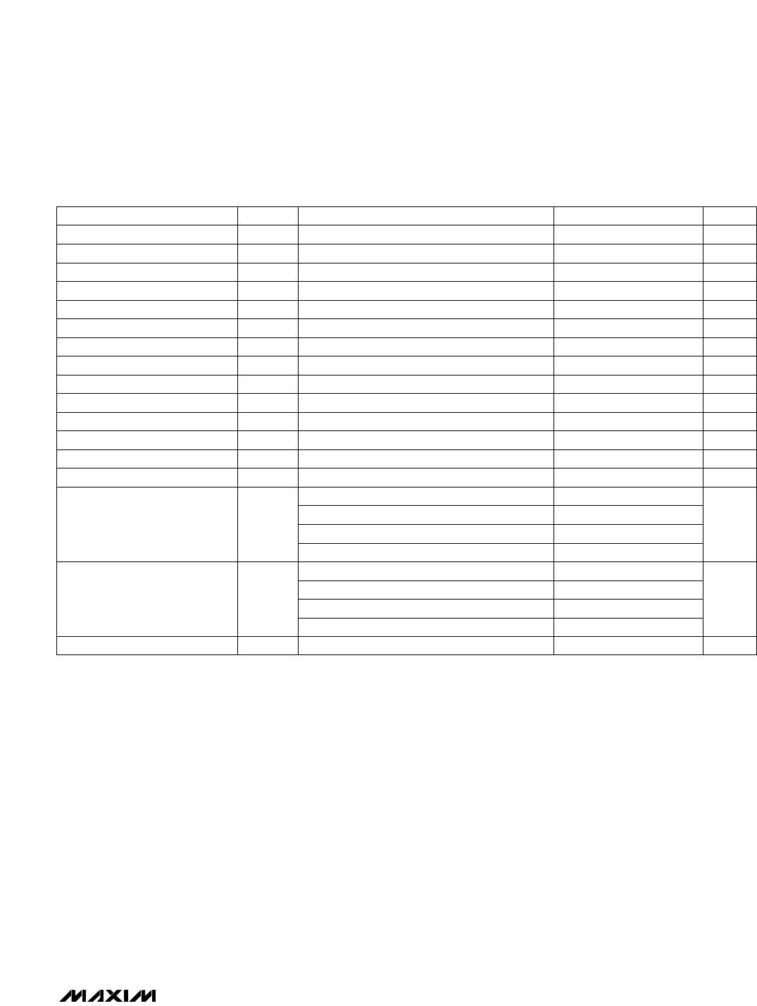
CONDITIONS UNITSMIN TYP MAXSYMBOLPARAMETER
I
OUT
= 1mA V4V
OH
Output High Voltage
I
OUT
= -1.6mA V0.4V
OL
Output Low Voltage
D0–D13 µA±10Three-State Leakage Current
(Note 7) pF10
Three-State Output
Capacitance
V4.75 5 5.25AV
DD
Positive Supply Voltage
V-5.25 -5 -4.75AV
SS
Negative Supply Voltage
V4.75 5 5.25DV
DD
Digital Supply Voltage
mA17 25I(AV
DD
)Positive Supply Current
mA-17 -13I(AV
SS
)Negative Supply Current
mA3 5I(DV
DD
)Digital Supply Current
mA3Shutdown Positive Current
mA-1Shutdown Negative Current
mA3Shutdown Digital Current
(Note 11) LSB±1 ±2PSRR+Positive Supply Rejection
(Note 11) LSB±2PSRR-Negative Supply Rejection
(Note 12) mW165 250Power Dissipation
DIGITAL OUTPUTS (D0–D13, INT) (Note 1)
POWER REQUIREMENTS
ELECTRICAL CHARACTERISTICS (continued)
(AV
DD
= +5V ±5%, AV
SS
= -5V ±5%, DV
DD
= +5V ±5%, V
REFIN
= 2.5V, AGND = DGND = 0V, 4.7µF capacitor from REFOUT to
AGND, 0.1µF capacitor from REFIN to AGND, f
CLK
= 16MHz, external clock, 50% duty cycle, T
A
= T
MIN
to T
MAX
, unless otherwise
noted.)
MAX125/MAX126
2x4-Channel, Simultaneous-Sampling
14-Bit DAS
_______________________________________________________________________________________ 5
CONDITIONS
ns30t
CW
CONVST Pulse Width
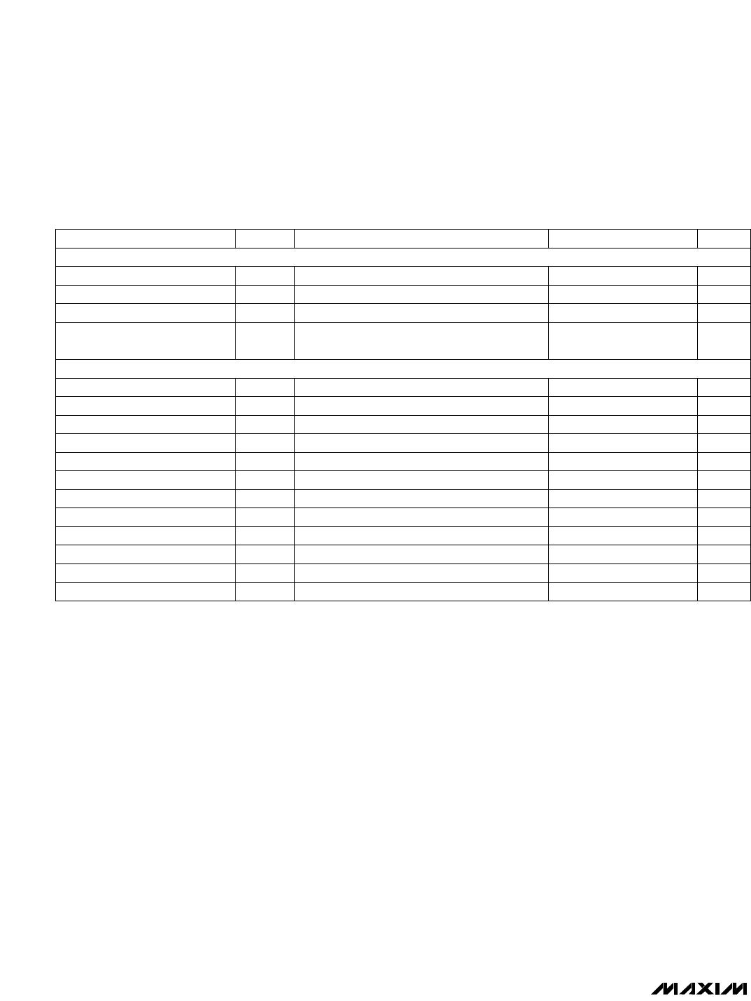
UNITSMIN TYP MAXSYMBOLPARAMETER
TIMING CHARACTERISTICS (Figure 4)
(AV
DD
= +5V, AV
SS
= -5V, DV
DD
= +5V, AGND = DGND = 0V, T
A
= T
MIN
to T
MAX
, unless otherwise noted.)
ns0t
CWS
CS to WR Setup Time
ns0t
CWH
CS to WR Hold Time
ns30t
WR
WR Low Pulse Width
ns125t
CSD
CS to CONVST Delay
ns30t
AS
Address Setup Time
ns0t
AH
Address Hold Time
25pF load ns30t
ID
RD to INT Delay
ns40t
RD
Delay Time Between Reads
ns0t
CRS
CS to RD Setup Time
ns0t
CRH
CS to RD Hold Time
ns30t
RD
RD Low Pulse Width
25pF load (Note 13) ns30t
DA
Data-Access Time
25pF load (Note 14) ns5 45t
DH
Bus-Relinquish Time
Mode 1, 1 channel
µs
3
Mode 2, 2 channel 6
Mode 3, 3 channel 9
Mode 4, 4 channel 12
t
CONV
Exiting shutdown µs5Start-Up Time
Note 1: AV
DD
= +5V, AV
SS
= -5V, DV
DD
= +5V, V
REFIN
= 2.500V (external), V
IN
= ±5V (MAX125) or ±2.5V (MAX126).
Note 2: Relative accuracy is the analog value’s deviation at any code from its theoretical value after the full-scale range has been
calibrated.
Note 3: CLK synchronized with CONVST.
Note 4: f
IN
= 10.06kHz, V
IN
= ±5V (MAX125) or ±2.5V (MAX126).
Note 5: First five harmonics.
Note 6: All inputs except CH1A driven with ±5V (MAX125) or ±2.5V (MAX126) 10kHz signal; CH1A connected to AGND and digitized.
Note 7: Guaranteed by design. Not production tested.
Note 8: AV
DD
= +5V, AV
SS
= -5V, DV
DD
= +5V, V
IN
= 0V (all channels).
Note 9: Temperature drift is defined as the change in output voltage from +25°C to T
MIN
or T
MAX
. It is calculated as
TC = [REFOUT/REFOUT] / T.
Note 10: See Figure 2.
Note 11: Defined as the change in positive full scale caused by a ±5% variation in the nominal supply voltage. Tested with one input
at full scale and all others at AGND. V
REFIN
= 2.5V (internal).
Note 12: Tested with V
IN
= AGND on all channels, V
REFIN
= 2.5V (internal).
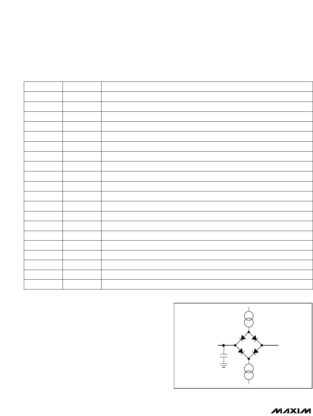
Note 13: The data-access time is defined as the time required for an output to cross 0.8V or 2.0V. It is measured using the circuit of
Figure 1. The measured number is then extrapolated back to determine the value with a 25pF load.
Note 14: The bus-relinquish time is derived from the measured time taken for the data outputs to change 0.5V when loaded with the
circuit of Figure 1. The measured number is then extrapolated back to remove the effects of charging/discharging the 120pF
capacitor. Thus, the time given is the part’s true bus-relinquish time, independent of the external bus loading capacitance.
Conversion Time
Mode 1, 1 channel
ksps
250
Conversion Rate/Channel
Mode 2, 2 channel 142
Mode 3, 3 channel 100
Mode 4, 4 channel 76
_______________Detailed Description
The MAX125/MAX126 use a successive-approximation
conversion technique and four simultaneous-sampling
track/hold (T/H) amplifiers to convert analog signals into
14-bit digital outputs. Each T/H has two multiplexed
inputs, allowing a total of eight inputs. Each T/H output
is converted and stored in memory to be accessed
sequentially by the parallel interface with successive
read cycles. The MAX125/MAX126 internal micro-
sequencer can be programmed to digitize one, two,
three, or four inputs sampled simultaneously from either
of the two banks of four inputs (see Figure 2).
The conversion timing and control sequences are
derived from a 16MHz external clock, the CONVST
MAX125/MAX126
2x4-Channel, Simultaneous-Sampling
14-Bit DAS
6 _______________________________________________________________________________________
NAME FUNCTION
1, 2 CH2B, CH2A Channel 2 Multiplexed Inputs, single-ended
3, 4 CH1B, CH1A Channel 1 Multiplexed Inputs, single-ended
PIN
5 AV
DD
+5V ±5% Analog Supply Voltage
6 REFIN External Reference Input/Internal Reference Output. Bypass with a 0.1µF capacitor to AGND.
17 DV
DD
+5V ±5% Digital Supply Voltage
916 D13–D6 Data Bits. D13 = MSB.
8, 36 AGND Analog Ground. Both pins must be tied to ground.
7 REFOUT Reference-Buffer Output. Bypass with a 4.7µF capacitor to AGND.
26
CS
Chip-Select Input (active-low)
25 CLK Clock Input (duty cycle must be 30% to 70%).
21–24 D3/A3–D0/A0 Bidirectional Data Bits/Address Bits. D0/A0 = LSB.
19, 20 D5, D4 Data Bits
18 DGND Digital Ground
______________________________________________________________Pin Description
27
WR
Write Input (active-low)
28
RD
Read Input (active-low)
29
CONVST
Conversion-Start Input. Rising edge initiates sampling and conversion sequence.
30
INT
Interrupt Output. Falling edge indicates the end of a conversion sequence.
31 AV
SS
-5V ±5% Analog Supply Voltage
32, 33 CH4A, CH4B Channel 4 Multiplexed Inputs, single-ended
34, 35 CH3A, CH3B Channel 3 Multiplexed Inputs, single-ended
Figure 1. Load Circuit for Access Time and Bus Relinquish Time
TO OUTPUT
PIN
120pF
1.0mA
1.6mA
1.6V

MAX125CEAX+D

Mfr. #:
Manufacturer:
Maxim Integrated
Description:
Analog to Digital Converters - ADC 14-Bit 8Ch 250ksps 2.75V Precision ADC
Lifecycle:
New from this manufacturer.
Delivery:
DHL FedEx Ups TNT EMS
Payment:
T/T Paypal Visa MoneyGram Western Union