MAX125/MAX126
2x4-Channel, Simultaneous-Sampling
14-Bit DAS
_______________________________________________________________________________________ 7
MUX
2.50V
BANDGAP REFERENCE
REFIN
10k
AGND REFOUT
MUX
T/H
T/H
T/H
T/H
A
B
MUX
A
B
MUX
A
B
MUX
CH1A
CH1B
CH2A
CH2B
CH3A
CH3B
CH4A
CH4B
A
B
14-BIT
DAC
CONTROL LOGIC
BUS INTERFACE
CLK CONVST INT CS RD WR DV
DD
DGND
SAR
14x4
RAM
V
REF
THREE-STATE
OUTPUT
DRIVERS
AV
DD
AGND
AV
SS
D0/A0 (LSB)
D1/A1
D2/A2
D3/A3
D13 (MSB)
MAX125
MAX126
V
REF
COMP
Figure 2. Functional Diagram
MAX125/MAX126
2x4-Channel, Simultaneous-Sampling
14-Bit DAS
8 _______________________________________________________________________________________
signal, and the programmed mode. The T/H amplifiers
hold the input voltages at the CONVST rising edge.
Additional CONVST pulses are ignored until the last
conversion for the sample is complete. The ADC con-
verts each assigned channel in 3µs and stores the
result in an internal 4x14-bit memory.
At the end of the last conversion, INT goes low and the
T/H amplifiers begin to track the inputs again. The data
can be accessed by applying successive pulses to the
RD pin. Successive reads access data words sequen-
tially. The memory is
not
random-access; data from
CH1 is always read first. After accessing all pro-
grammed channels, the address pointer selects CH1
again. Additional read pulses cycle through the data
words. CS can be held low during successive reads.
Input Bandwidth
The T/H’s input tracking circuitry has an 8MHz small-
signal bandwidth, so it is possible to digitize high-
speed transient events and measure periodic signals
with bandwidths exceeding the ADC’s sampling rate by
using undersampling techniques. To avoid high-
frequency signals being aliased into the frequency
band of interest, anti-alias filtering is recommended.
Analog Input Range and Input Protection
The MAX125’s input range is ±5V, and the MAX126’s
input range is ±2.5V. The input resistance for both parts
is 10k. An input protection structure allows input volt-
ages to ±17V without harming the IC. This protection is
also active in shutdown mode.
Track/Holds
The MAX125/MAX126 feature four simultaneous T/Hs.
Each T/H has two multiplexed inputs. A T-switch input
configuration provides excellent hold-mode isolation.
Allow 1µs acquisition time for 14-bit accuracy.
The T/H aperture delay is typically 10ns. The 500ps
aperture-delay mismatch between the T/Hs allows the
relative phase information of up to four different inputs
to be preserved. Figure 3 shows the equivalent input
circuit, illustrating the ADC’s sampling architecture.
Only one of four T/H stages with its two multiplexed
inputs (CH_A and CH_B) is shown. All switches are in
track configuration for channel A. An internal buffer
charges the hold capacitor to minimize the required
acquisition time between conversions. The analog input
appears as a 10kresistor in parallel with a 16pF
capacitor.
Figure 3. Equivalent Input Circuit
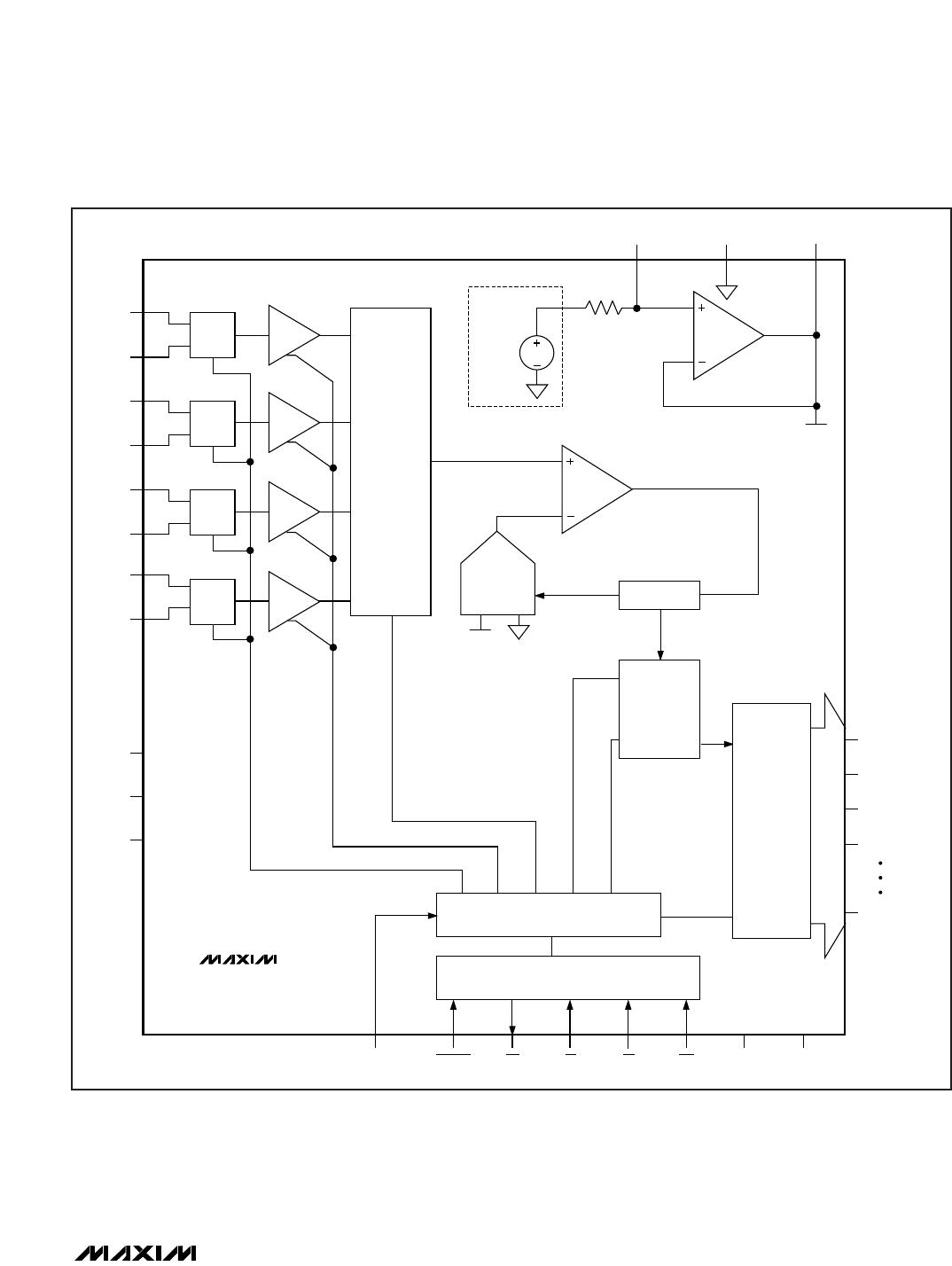
Between conversions, the buffer input is connected to
channel 1 of the selected track/hold bank. When a
channel is not selected, switches S1, S2, and S3 are
placed in hold mode to improve channel-to-channel
isolation.
Digital Interface
Input data (A0–A3) and output data (D0–D13) are multi-
plexed on a three-state bidirectional interface. This par-
allel I/O can easily be interfaced with a microprocessor
P) or DSP. CS, WR, and RD control the write and read
operations. CS is the standard chip-select signal, which
enables the controller to address the MAX125/MAX126
as an I/O port. When CS is high, it disables the WR and
RD inputs and forces the interface into a high-Z state.
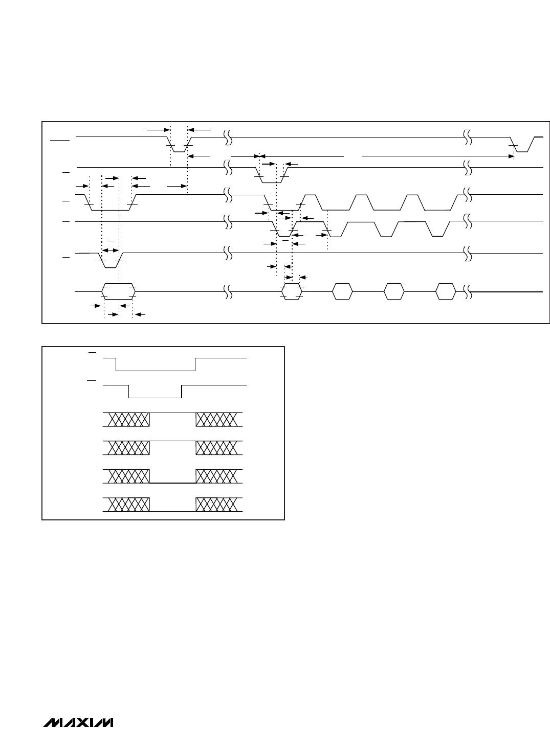
Figure 4 details the interface timing.
Programming Modes
The MAX125/MAX126 have eight conversion modes
plus power-down, which are programmed through a
bidirectional parallel interface. At power-up, the devices
default to the mode
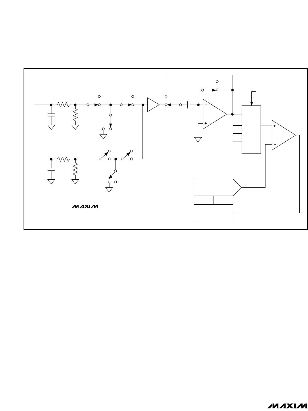
Input Mux A/Single-Channel
Conversion.
The user can select between two banks
(mux inputs A or mux inputs B) of four simultaneous-
sampled input channels, as illustrated in Figure 2. An
internal microsequencer can be programmed to convert
one, two, three, or four channels of the selected bank
per sample. For a single-channel conversion, CH1 is
digitized, and then INT goes low to indicate completion
of the conversion. For multichannel conversions, INT
goes low after the last channel has been digitized.
To input data into the MAX125/MAX126, pull CS low,
program the bidirectional pins A0–A3 (Table 1), and
pulse WR low. Data is latched into the devices on the
WR or CS rising edge. The ADC is now ready to convert.
Once programmed, the ADCs continue operating in the
same mode until they are reprogrammed or until power
is removed. Figure 5 shows an example of program-
ming a four-channel conversion using Input Mux A.
Starting a Conversion
After programming the MAX125/MAX126 as outlined in
the
Programming Modes
section, pulse CONVST low to
initiate a conversion sequence. The analog inputs are
sampled at the CONVST rising edge. Do not start a
new conversion while the conversion is in progress.
Monitor the INT output. A falling edge indicates the end
of a conversion sequence.
MAX125/MAX126
2x4-Channel, Simultaneous-Sampling
14-Bit DAS
_______________________________________________________________________________________ 9
CH1 CH2 CH3 CH4
t
ACQ
t
CONV
t
AH
t
AS
t
WR
t
CSD
t
CWH
t
DH
t
DA
t
RD
t
CRS
t
CRH
t
RD
t
ID
t
CWS
CONVST
INT
CS
WR
DATA
t
CW
DATA IN
RD
Figure 4. Timing Diagram
Figure 5. Programming a Four-Channel Conversion, Input Mux A
A0
(LSB)
WR
CS
A1
A2
A3

MAX125CEAX+D

Mfr. #:
Manufacturer:
Maxim Integrated
Description:
Analog to Digital Converters - ADC 14-Bit 8Ch 250ksps 2.75V Precision ADC
Lifecycle:
New from this manufacturer.
Delivery:
DHL FedEx Ups TNT EMS
Payment:
T/T Paypal Visa MoneyGram Western Union