2:4 3.3V PCIE CLOCK MUX 4 REVISION A 06/06/16
9DML04 DATASHEET
Test Loads
Alternate Terminations
The 9DML family can easily drive LVPECL, LVDS, and CML logic. See “AN-891 Driving LVPECL, LVDS, and CML Logic with
IDT's "Universal" Low-Power HCSL Outputs” for details.
Rs
Rs
Low-Power HCSL Differential Output Test Load
2pF 2pF
5 inches
Zo (
Device
Terminations
Device Zo ()Rs ()
9DML0441 100 None needed
9DML0451 100 7.5
9DML04P1 100 Prog.
9DML0441 85 N/A
9DML0451 85 None needed
9DML04P1 85 Prog.
REVISION A 06/06/16 5 2:4 3.3V PCIE CLOCK MUX
9DML04 DATASHEET
Absolute Maximum Ratings
Stresses above the ratings listed below can cause permanent damage to the 9DML04. These ratings, which are standard values
for IDT commercially rated parts, are stress ratings only. Functional operation of the device at these or any other conditions
above those indicated in the operational sections of the specifications is not implied. Exposure to absolute maximum rating
conditions for extended periods can affect product reliability. Electrical parameters are guaranteed only over the recommended
operating temperature range.
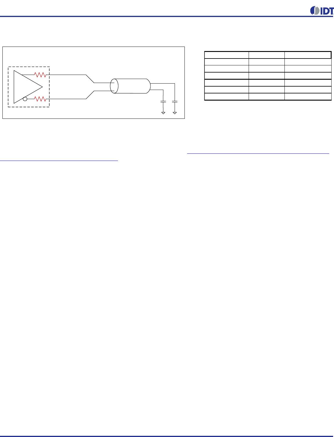
Electrical Characteristics–Clock Input Parameters
Electrical Characteristics–Current Consumption
PARAMETER SYMBOL CONDITIONS
MIN TYP MAX
UNITS NOTES
Supply Voltage VDDx 4.6 V 1,2
Input Voltage V
IN
-0.5 V
D
D
+0.5 V 1,3
Input High Voltage, SMBus V
IHSMB
SMBus clock and data pins 3.9 V 1
Storage Temperature Ts -65 150 °C 1
Junction Temperature Tj 125 °C 1
Input ESD protection
ESD prot Human Body Model 2500 V 1
1
Guaranteed by design and characterization, not 100% tested in production.
2
Operation under these conditions is neither implied nor guaranteed.
3
Not to exceed 4.6V.
TA = T
AMB,
Supply Voltages per normal operation conditions, See Test Loads for Loading Conditions
PARAMETER SYMBOL CONDITIONS MIN TYP MAX UNITS NOTES
Input Common Mode
Voltage - DIF_IN
V
COM
Common Mode Input Voltage 150 900 mV 1
Input Swing - DIF_IN V
SWING
Differential value 300 mV 1
Input Slew Rate - DIF_IN dv/dt Measured differentially 0.4 8 V/ns 1,2
Input Leakage Current I
IN
V
IN
= V
DD ,
V
IN
=
GND -5 5 uA
Input Duty Cycle d
tin
Measurement from differential wavefrom 45 55 % 1
Input Jitter - Cycle to Cycle J
DIFIn
Differential Measurement 0 125 ps 1
1
Guaranteed by design and characterization, not 100% tested in production.
2
Slew rate measured through +/-75mV window centered around differential zero
TA = T
AMB,
Supply Voltages per normal operation conditions, See Test Loads for Loading Conditions
PARAMETER SYMBOL CONDITIONS MIN TYP MAX UNITS NOTES
Operating Supply Current
I
D
D
VDD, All outputs active @100MHz
23 30
mA
Powerdown Current
I
DDPD
VDD, all outputs disabled 1.6 2.5 mA
1
1
Input clock stopped.
2:4 3.3V PCIE CLOCK MUX 6 REVISION A 06/06/16
9DML04 DATASHEET
Electrical Characteristics–Input/Supply/Common Parameters–Normal Operating
Conditions
TA = T
AMB,
Supply Voltages per normal operation conditions, See Test Loads for Loading Conditions
PARAMETER SYMBOL CONDITIONS MIN TYP MAX UNITS NOTES
Supply Voltage VDDx Supply voltage for core and analog 3.135 3.3 3.465 V
Ambient Operating
Temperature
T
AMB
Industrial range -40 25 85 °C
Input High Voltage V
IH
Single-ended inputs, except SMBus 0.75 V
DD
V
DD
+ 0.3 V
Input Low Voltage V
IL
Single-ended inputs, except SMBus -0.3 0.25 V
D
D
V
I
IN
Single-ended inputs, V
IN
= GND, V
IN
= VDD -5 5 uA
I
INP
Single-ended inputs
V
IN
= 0 V; Inputs with internal pull-up resistors
V
IN
= VDD; Inputs with internal pull-down resistors
-50 50 uA
Input Frequency F
ib
yp
1 200 MHz 2
Pin Inductance L
p
in
7nH1
C
IN
Logic Inputs, except DIF_IN 1.5 5 pF 1
C
INDIF_IN
DIF_IN differential clock inputs 1.5 2.7 pF 1
C
OUT
Output pin capacitance 6 pF 1
Clk Stabilization T
STAB
From V
DD
Power-Up and after input clock
stabilization or de-assertion of PD# to 1st clock
0.7 1 ms 1,2
Input SS Modulation
Frequency PCIe
f
MODI NPCIe
Allowable Frequency for PCIe Applications
(Triangular Modulation)
30 31.5 33 kHz
Input SS Modulation
Frequency non-PCIe
f
MODIN
Allowable Frequency for non-PCIe Applications
(Triangular Modulation)
066kHz
OE# Latency t
LATOE#
DIF start after OE# assertion
DIF stop after OE# deassertion
123clocks1,3
Tdrive_PD# t
DRVPD
DIF output enable after
PD# de-assertion
300 us 1,3
Tfall t
F
Fall time of single-ended control inputs 5 ns 2
Trise t
R
Rise time of single-ended control inputs 5 ns 2
1
Guaranteed by design and characterization, not 100% tested in production.
2
Control input must be monotonic from 20% to 80% of input swin
g
.
3
Time from deassertion until outputs are >200 mV
4
The differential input clock must be running for the SMBus to be active
Input Current
Capacitance

9DML0451AKILFT

Mfr. #:
Manufacturer:
IDT
Description:
Clock Buffer 2:4 LP-HCSL CLOCK MUX ZO=85OHM
Lifecycle:
New from this manufacturer.
Delivery:
DHL FedEx Ups TNT EMS
Payment:
T/T Paypal Visa MoneyGram Western Union

Products related to this Datasheet