REVISION A 06/06/16 7 2:4 3.3V PCIE CLOCK MUX
9DML04 DATASHEET
Electrical Characteristics–DIF Low-Power HCSL Outputs
Electrical Characteristics–Output Duty Cycle, Jitter, Skew and PLL Characteristics
TA = T
AMB,
Supply Voltages per normal operation conditions, See Test Loads for Loading Conditions
PARAMETER SYMBOL CONDITIONS MIN TYP MAX UNITS NOTES
Slew rate dV/dt Scope averaging on, default settings 1.5 2.6 4
V/ns
1,2,3
Slew rate matchin
g
Δ
dV/dt Slew rate matchin
g
8.6 20
%
1,2,4
Voltage High V
HIGH
660 780 850 7
Voltage Low V
LOW
-150 -32 150 7
Max Volta
g
e Vmax 835 1150 7
Min Voltage Vmin -300 -90 7
Crossing Voltage (abs) Vcross_abs Scope averaging off 250 406 550 mV 1,5
Crossing Voltage (var)
Δ
-Vcross Scope averaging off 20 140 mV 1,6
2
Measured from differential waveform
7
These are defaults for the 41/51 devices. They are factory adjustable in the P1 device.
Statistical measurement on single-ended signal
using oscilloscope math function. (Scope
averaging on)
mV
Measurement on single ended signal using
absolute value. (Scope averaging off)
mV
1
Guaranteed by design and characterization, not 100% tested in production.
3
Slew rate is measured through the Vswing voltage range centered around differential 0V. This results in a +/-150mV window around
differential 0V. These are defaults for the 41/51 devices, alternate settings are available in the P1 device.
4
Matching applies to rising edge rate for Clock and falling edge rate for Clock#. It is measured using a +/-75mV window centered on
the average cross point where Clock rising meets Clock# falling. The median cross point is used to calculate the voltage thresholds the
oscilloscope is to use for the edge rate calculations.
5
Vcross is defined as voltage where Clock = Clock# measured on a component test board and only applies to the differential rising
edge (i.e. Clock rising and Clock# falling).
6
The total variation of all Vcross measurements in any particular system. Note that this is a subset of Vcross_min/max (Vcross
absolute) allowed. The intent is to limit Vcross induced modulation by setting
Δ
-Vcross to be smaller than Vcross absolute.
TA = T
AMB,
Supply Voltages per normal operation conditions, See Test Loads for Loading Conditions
PARAMETER SYMBOL CONDITIONS MIN TYP MAX UNITS NOTES
Duty Cycle Distortion t
DC
D
Measured differentially, @100MHz -0.5 0.3 1.2 % 1,3
Skew, Input to Output t
p
d
V
T
= 50% 2600 3428 4500 ps 1
Skew, Output to Output t
sk3
V
T
= 50% 23 50 ps 1
Jitter, Cycle to cycle t
jcyc-cyc
Additive Jitter in Bypass Mode 0.1 1 ps 1,2
1
Guaranteed by design and characterization, not 100% tested in production.
2
Measured from differential waveform
3
Duty cycle distortion is the difference in duty cycle between the output and the input clock.
2:4 3.3V PCIE CLOCK MUX 8 REVISION A 06/06/16
9DML04 DATASHEET
Electrical Characteristics–Filtered Phase Jitter Parameters - PCIe Common Clocked
(CC) Architectures
Electrical Characteristics–Filtered Phase Jitter Parameters - PCIe Separate
Reference Independent Spread (SRIS) Architectures
5
Electrical Characteristics– Unfiltered Phase Jitter Parameters
T
AMB
= over the specified operating range. Supply Voltages per normal operation conditions, See Test Loads for Loading Conditions
PARAMETER SYMBOL CONDITIONS MIN TYP MAX
INDUSTRY
LIMIT
UNITS Notes
t
jphPCIeG1-CC
PCIe Gen 1 0.0 0.01
ps
(p-p)
1,2,3,5
PCIe Gen 2 Lo Band
10kHz < f < 1.5MHz
(PLL BW of 5-16MHz or 8-5MHz, CDR = 5MHz)
0.0 0.01
ps
(rms)
1,2,4,5
PCIe Gen 2 High Band
1.5MHz < f < Nyquist (50MHz)
(PLL BW of 5-16MHz or 8-5MHz, CDR = 5MHz)
0.0 0.01
ps
(rms)
1,2,4,5
t
jphPCIeG3-CC
PCIe Gen 3
(PLL BW of 2-4MHz or 2-5MHz, CDR = 10MHz)
0.0 0.01
ps
(rms)
1,2,4,5
t
jphPCIeG4-CC
PCIe Gen 4
(PLL BW of 2-4MHz or 2-5MHz, CDR = 10MHz)
0.0 0.01
ps
(rms)
1,2,4,5
1
Applies to all outputs.
5
Driven by 9FGL0841 or equivalent
Additive Phase Jitter n/a
t
jphPCIeG2-CC
2
Based on PCIe Base Specification Rev4.0 version 0.7draft. See http://www.pcisig.com for latest specifications.
3
Sample size of at least 100K cycles. This figures extrapolates to 108ps pk-pk @ 1M cycles for a BER of 1-12.
4
For RMS values additive jitter is calculated by solving the following equation for b [a^2+b^2=c^2 ] where a is rms input jitter and c is rms total
T
AMB
= over the specified operating range. Supply Voltages per normal operation conditions, See Test Loads for Loading Conditions
PARAMETER SYMBOL CONDITIONS MIN TYP MAX
INDUSTRY
LIMIT
UNITS Notes
t
jphPCIeG2-
SRIS
PCIe Gen 2
(PLL BW of 16MHz , CDR = 5MHz)
0.0 0.01
ps
(rms)
1,2,4
t
jphPCIeG3-
SRIS
PCIe Gen 3
(PLL BW of 2-4MHz or 2-5MHz, CDR = 10MHz)
0.0
0.01
ps
(rms)
1,2,4
1
Applies to all outputs.
Additive Phase Jitter n/a
2
Based on PCIe Base Specification Rev3.1a. These filters are different than Common Clock filters. See http://www.pcisig.com for latest
3
Sample size of at least 100K cycles. This figures extrapolates to 108ps pk-pk @ 1M cycles for a BER of 1-12.
4
For RMS values, additive jitter is calculated by solving the following equation for b [a^2+b^2=c^2 ] where a is rms input jitter and c is rms total
5
As of PCIe Base Specification Rev4.0 draft 0.7, SRIS is not currently defined for Gen1 or Gen4.
TA = T
AMB,
Supply Voltages per normal operation conditions, See Test Loads for Loading Conditions
PARAMETER SYMBOL CONDITIONS MIN TYP MAX
INDUSTRY
LIMIT UNITS Notes
t
jph156M
156.25MHz, 1.5MHz to 10MHz, -20dB/decade
rollover < 1.5MHz, -40db/decade rolloff > 10MHz
159 N/A
fs
(rms)
1,2,3
t
jph156M12k-
20
156.25MHz, 12kHz to 20MHz, -20dB/decade
rollover <12kHz, -40db/decade rolloff > 20MHz
363 N/A
fs
(rms)
1,2,3
1
Guaranteed by design and characterization, not 100% tested in production.
3
For RMS figures, additive jitter is calculated by solving the following equation: Additive jitter = SQRT[(total jitter)^2 - (input jitter)^2]
2
Driven by Rohde&Schartz SMA100
Additive Phase Jitter,
Fanout Mode
REVISION A 06/06/16 9 2:4 3.3V PCIE CLOCK MUX
9DML04 DATASHEET
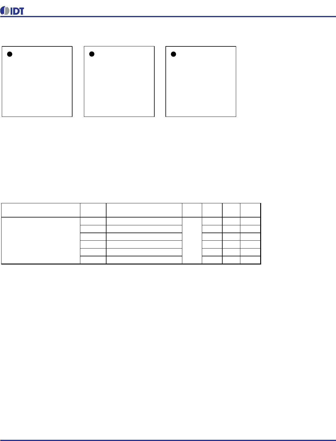
Marking Diagrams
Notes:
1. “LOT” is the lot sequence number.
2. “YYWW” or “YWW” is the digits of the year and week that the part was assembled.
3. “I” denotes industrial temperature range device.
4. “P” denotes factory programmable defaults.
5. “**” denotes the lot sequence.
6. “$” denotes the mark code.
Thermal Characteristics
LOT
441AI
YYWW
LOT
451AI
YYWW
4P1AI
000
YWW**$
PARAMETER SYMBOL CONDITIONS PKG
TYP
VALUE
UNITS NOTES
θ
JC
Junction to Case 42 °
C/W
1
θ
Jb
Junction to Base 2.4 °
C/W
1
θ
JA0
Junction to Air, still air 39 °
C/W
1
θ
JA1
Junction to Air, 1 m/s air flow 33 °
C/W
1
θ
JA3
Junction to Air, 3 m/s air flow 28 °
C/W
1
θ
JA5
Junction to Air, 5 m/s air flow 27 °
C/W
1
1
ePad soldered to board
Thermal Resistance NLG24

9DML0451AKILFT

Mfr. #:
Manufacturer:
IDT
Description:
Clock Buffer 2:4 LP-HCSL CLOCK MUX ZO=85OHM
Lifecycle:
New from this manufacturer.
Delivery:
DHL FedEx Ups TNT EMS
Payment:
T/T Paypal Visa MoneyGram Western Union

Products related to this Datasheet