AMPLITUDE – dB
INPUT FREQUENCY – kHz
10000
–100
–120
101
–60
–80
–40
–20
0
1000
THD
2
ND
HARMONIC
3
RD
HARMONIC
f
SAMPLE
= 100kSPS
FULL-SCALE = +10V
100
Figure 5. Harmonic Distortion vs.
Input Frequency
Typical Dynamic Performance–AD1674
GENERAL CIRCUIT OPERATION
The AD1674 is a complete 12-bit, 10 µs sampling analog-to-
digital converter. A block diagram of the AD1674 is shown on
page 7.
When the control section is commanded to initiate a conversion
(as described later), it places the sample-and-hold amplifier
(SHA) in the hold mode, enables the clock, and resets the suc-
cessive approximation register (SAR). Once a conversion cycle
has begun, it cannot be stopped or restarted and data is not
available from the output buffers. The SAR, timed by the inter-
nal clock, will sequence through the conversion cycle and return
an end-of-convert flag to the control section when the conver-
sion has been completed. The control section will then disable
the clock, switch the SHA to sample mode, and delay the STS
LOW going edge to allow for acquisition to 12-bit accuracy.
The control section will allow data read functions by external
command anytime during the SHA acquisition interval.
During the conversion cycle, the internal 12-bit, 1 mA full-scale
current output DAC is sequenced by the SAR from the most
significant bit (MSB) to the least significant bit (LSB) to pro-
vide an output that accurately balances the current through the
5 k resistor from the input signal voltage held by the SHA.
The SHA’s input scaling resistors divide the input voltage by 2
for the 10 V input span and by 4 V for the 20 V input span,
maintaining a 1 mA full-scale output current through the 5 k
resistor for both ranges. The comparator determines whether
the addition of each successively weighted bit current causes the
DAC current sum to be greater than or less than the input cur-
rent. If the sum is less, the bit is left on; if more, the bit is
turned off. After testing all the bits, the SAR contains a 12-bit
binary code which accurately represents the input signal to
within ±1/2 LSB.
CONTROL LOGIC
The AD1674 may be operated in one of two modes, the full-
control mode and the stand-alone mode. The full-control mode
utilizes all the AD1674 control signals and is useful in systems
that address decode multiple devices on a single data bus. The
stand-alone mode is useful in systems with dedicated input ports
available and thus not requiring full bus interface capability.
Table I is a truth table for the AD1674, and Figure 10 illus-
trates the internal logic circuitry.
Table I. AD1674A Truth Table
CE CS R/C 12/8 A
0
Operation
0 X X X X None
X 1 X X X None
1 0 0 X 0 Initiate 12-Bit Conversion
1 0 0 X 1 Initiate 8-Bit Conversion
1 0 1 1 X Enable 12-Bit Parallel Output
1 0 1 0 0 Enable 8 Most Significant Bits
1 0 1 0 1 Enable 4 LSBs +4 Trailing Zeroes
REV. C
–9–
Figure 7. S/(N+D) vs. Input Amplitude
0
–130
50
–100
–120
5
–110
0
–70
–90
–80
–60
–40
–30
–10
–20
–50
4535301510
FREQUENCY – kHz
AMPLITUDE – dB
20 25 40
Figure 9. IMD Plot for f
IN
= 9.08 kHz (fa), 9.58 kHz (fb)
0
–140
50
–80
–120
5
–100
0
–20
–60
–40
4540353025201510
FREQUENCY – kHz
AMPLITUDE – dB
Figure 8. Nonaveraged 2048 Point FFT
at 100 kSPS, f
IN
= 25.049 kHz
INPUT FREQUENCY – kHz
S/(N+D) – dB
80
0
10000
20
10
101
40
30
50
60
70
1000
0dB INPUT
–20dB INPUT
–60dB INPUT
100
Figure 6. S/(N+D) vs. Input Frequency
and Amplitude
AD1674
REV. C
–10–
Q
R
S
READ
S
R
Q
QB
VALUE OF A
0
AT LAST
CONVERT COMMAND
EOC 12
EOC 8
SAR RESET
1µs DELAY-HOLD SETTLING
1µs DELAY-ACQUISITION
NYBBLE A
NYBBLE B
NYBBLE C
NYBBLE B = 0
TO OUTPUT
BUFFERS
CE
A
0
12/8
R/C
CS
D
Q
QB
EN
D
Q
EN
CLK ENABLE
STATUS
HOLD/SAMPLE
Figure 10. Equivalent Internal Logic Circuitry
FULL-CONTROL MODE
Chip Enable (CE), Chip Select (
CS) and Read/ Convert (R/C)
are used to control Convert or Read modes of operation. Either
CE or
CS may be used to initiate a conversion. The state of R/C
when CE and
CS are both asserted determines whether a data
Read (R/
C = 1) or a Convert (R/C = 0) is in progress. R/C
should be LOW before both CE and
CS are asserted; if R/C is
HIGH, a Read operation will momentarily occur, possibly
resulting in system bus contention.
STAND-ALONE MODE
The AD1674 can be used in a “stand-alone” mode, which is
useful in systems with dedicated input ports available and thus
not requiring full bus interface capability. Stand-alone mode
applications are generally able to issue conversion start com-
mands more precisely than full-control mode. This improves ac
performance by reducing the amount of control-induced aper-
ture jitter.
In stand-alone mode, the control interface for the AD1674 and
AD674A are identical. CE and 12/
8 are wired HIGH, CS and
A
0
are wired LOW, and conversion is controlled by R/C. The
three-state buffers are enabled when R/
C is HIGH and a con-
version starts when R/
C goes LOW. This gives rise to two pos-
sible control signals—a high pulse or a low pulse. Operation
with a low pulse is shown in Figure 4a. In this case, the outputs
are forced into the high impedance state in response to the fall-
ing edge of R/
C and return to valid logic levels after the conver-
sion cycle is completed. The STS line goes HIGH 200 ns after
R/
C goes LOW and returns low 1 µs after data is valid.
If conversion is initiated by a high pulse as shown in Figure 4b,
the data lines are enabled during the time when R/
C is HIGH.
The falling edge of R/
C starts the next conversion and the data
lines return to three-state (and remain three-state) until the next
high pulse of R/
C.
CONVERSION TIMING
Once a conversion is started, the STS line goes HIGH. Convert
start commands will be ignored until the conversion cycle is
complete. The output data buffers will be enabled a minimum
of 0.6 µs prior to STS going LOW. The STS line will return
LOW at the end of the conversion cycle.
The register control inputs, A
0
and 12/8, control conversion
length and data format. If a conversion is started with A
0
LOW,
a full 12-bit conversion cycle is initiated. If A
0
is HIGH during a
convert start, a shorter 8-bit conversion cycle results.
During data read operations, A
0
determines whether the three-
state buffers containing the 8 MSBs of the conversion result (A
0
= 0) or the 4 LSBs (A
0
= 1) are enabled. The 12/8 pin deter-
mines whether the output data is to be organized as two 8-bit
words (12/
8 tied LOW) or a single 12-bit word (12/8 tied
HIGH). In the 8-bit mode, the byte addressed when A
0
is high
contains the 4 LSBs from the conversion followed by four trail-
ing zeroes. This organization allows the data lines to be over-
lapped for direct interface to 8-bit buses without the need for
external three-state buffers.
INPUT CONNECTIONS AND CALIBRATION
The 10 V p-p and 20 V p-p full-scale input ranges of the
AD1674 accept the majority of signal voltages without the need
for external voltage divider networks which could deteriorate the
accuracy of the ADC.
The AD1674 is factory trimmed to minimize offset, linearity,
and full-scale errors. In many applications, no calibration trim-
ming will be required and the AD1674 will exhibit the accuracy
limits listed in the specification tables.
In some applications, offset and full-scale errors need to be
trimmed out completely. The following sections describe the
correct procedure for these various situations.
UNIPOLAR RANGE INPUTS
Figure 11 illustrates the external connections for the AD1674 in
unipolar-input mode. The first output-code transition (from
0000 0000 0000 to 0000 0000 0001) should nominally occur
for an input level of +1/2 LSB (1.22 mV above ground for a 10 V
range; 2.44 mV for a 20 V range). To trim unipolar offset to this
nominal value, apply a +1/2 LSB signal between Pin 13 and
ground (10 V range) or Pin 14 and ground (20 V range) and ad-
just R1 until the first transition is located. If the offset trim is
not required, Pin 12 can be connected directly to Pin 9; the two
resistors and trimmer for Pin 12 are then not needed.
AD1674
REV. C
–11–
100k
AD1674
R1
100k
–15V
+15V
R2
100
100
ANALOG
INPUTS
0 TO +20V
0 TO +10V
2 12/8
3 CS
4 A
0
5 R/C
6 CE
10 REF IN
8 REF OUT
12 BIP OFF
13 10V
IN
14 20V
IN
9 ANA COM
STS 28
HIGH BITS
24-27
MIDDLE BITS
20-23
LOW BITS
16-19
+5V 1
+15V 7
–15V 11
DIG COM 15
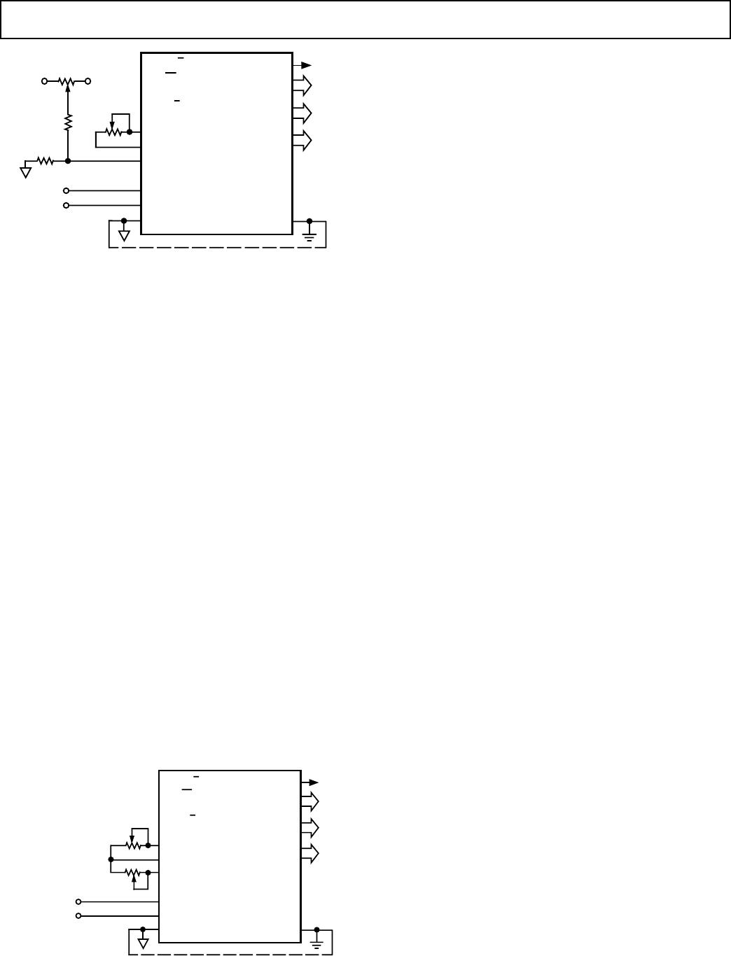
Figure 11. Unipolar Input Connections with Gain and
Offset Trims
The full-scale trim is done by applying a signal 1 1/2 LSB below
the nominal full scale (9.9963 V for a 10 V range) and adjusting
R2 until the last transition is located (1111 1111 1110 to 1111
1111 1111). If full-scale adjustment is not required, R2 should
be replaced with a fixed 50 ±1% metal film resistor. If REF
OUT is connected directly to REF IN, the additional full-scale
error will be approximately 1%.
BIPOLAR RANGE INPUTS
The connections for the bipolar-input mode are shown in Figure
12. Either or both of the trimming potentiometers can be
replaced with 50 ± 1% fixed resistors if the specified AD1674
accuracy limits are sufficient for the application. If the pins are
shorted together, the additional offset and gain errors will be
approximately 1%.
To trim bipolar offset to its nominal value, apply a signal 1/2
LSB below midrange (–1.22 mV for a ±5 V range) and adjust
R1 until the major carry transition is located (0111 1111 1111
to 1000 0000 0000). To trim the full-scale error, apply a signal
1 1/2 LSB below full scale (+4.9963 V for a ±5 V range) and
adjust R2 to give the last positive transition (1111 1111 1110 to
1111 1111 1111). These trims are interactive so several itera-
tions may be necessary for convergence.
A single-pass calibration can be done by substituting a negative
full-scale trim for the bipolar offset trim (error at midscale),
using the same circuit. First, apply a signal 1/2 LSB above minus
full scale (–4.9988 V for a ±5 V range) and adjust R1 until the
minus full-scale transition is located (0000 0000 0001 to 0000
0000 0000). Then perform the gain error trim as outlined above.
R1
100
±10V
±5V
AD1674
R2
100
ANALOG
INPUTS
2 12/8
3 CS
4 A
0
5 R/C
6 CE
10 REF IN
8 REF OUT
12 BIP OFF
13 10V
IN
14 20V
IN
9 ANA COM
STS 28
HIGH BITS
24-27
MIDDLE BITS
20-23
LOW BITS
16-19
+5V 1
+15V 7
–15V 11
DIG COM 15
Figure 12. Bipolar Input Connections with Gain and Offset
Trims
REFERENCE DECOUPLING
It is recommended that a 10 µF tantalum capacitor be con-
nected between REF IN (Pin 10) and ground. This has the
effect of improving the S/(N+D) ratio through filtering possible
broad-band noise contributions from the voltage reference.
BOARD LAYOUT
Designing with high resolution data converters requires careful
attention to board layout. Trace impedance is a significant issue.
At the 12-bit level, a 5 mA current through a 0.5 trace will
develop a voltage drop of 2.5 mV, which is 1 LSB for a 10 V
full-scale range. In addition to ground drops, inductive and ca-
pacitive coupling need to be considered, especially when high
accuracy analog signals share the same board with digital sig-
nals. Finally, power supplies should be decoupled in order to
filter out ac noise.
The AD1674 has a wide bandwidth sampling front end. This
means that the AD1674 will “see” high frequency noise at the
input, which nonsampling (or limited-bandwidth sampling)
ADCs would ignore. Therefore, it’s important to make an effort
to eliminate such high frequency noise through decoupling or by
using an anti-aliasing filter at the analog input of the AD1674.
Analog and digital signals should not share a common path.
Each signal should have an appropriate analog or digital return
routed close to it. Using this approach, signal loops enclose a
small area, minimizing the inductive coupling of noise. Wide PC
tracks, large gauge wire, and ground planes are highly recom-
mended to provide low impedance signal paths. Separate analog
and digital ground planes are also desirable, with a single inter-
connection point to minimize ground loops. Analog signals
should be routed as far as possible from digital signals and
should cross them (if necessary) only at right angles.
The AD1674 incorporates several features to help the user’s lay-
out. Analog pins are adjacent to help isolate analog from digital
signals. Ground currents have been minimized by careful circuit
architecture. Current through AGND is 2.2 mA, with little
code-dependent variation. The current through DGND is domi-
nated by the return current for DB11–DB0.
SUPPLY DECOUPLING
The AD1674 power supplies should be well filtered, well regu-
lated, and free from high frequency noise. Switching power sup-
plies are not recommended due to their tendency to generate
spikes which can induce noise in the analog system.
Decoupling capacitors should be used in very close layout prox-
imity between all power supply pins and ground. A 10 µF tanta-
lum capacitor in parallel with a 0.1 µF disc ceramic capacitor
provides adequate decoupling over a wide range of frequencies.
An effort should be made to minimize the trace length between
the capacitor leads and the respective converter power supply
and common pins. The circuit layout should attempt to locate
the AD1674, associated analog input circuitry, and interconnec-
tions as far as possible from logic circuitry. A solid analog
ground plane around the AD1674 will isolate large switching
ground currents. For these reasons, the use of wire-wrap circuit
construction is not recommended; careful printed-circuit con-
struction is preferred.

AD1674AR-REEL

Mfr. #:
Manufacturer:
Description:
Analog to Digital Converters - ADC 12-Bit 100 kSPS Complete IC
Lifecycle:
New from this manufacturer.
Delivery:
DHL FedEx Ups TNT EMS
Payment:
T/T Paypal Visa MoneyGram Western Union