REV. C
–3–
AD1674
AD1674A AD1674B AD1674T
Parameter Min Typ Max Min Typ Max Min Typ Max Unit
RESOLUTION 12 12 12 Bits
INTEGRAL NONLINEARITY (INL) ±1 ±1/2 ±1/2 LSB
±1 ±1/2 ±1 LSB
DIFFERENTIAL NONLINEARITY (DNL)
(No Missing Codes) 12 12 12 Bits
UNIPOLAR OFFSET
1
@ +25°C ±2 ±2 ±2 LSB
BIPOLAR OFFSET
1
@ +25°C ±6 ±3 ±3 LSB
FULL-SCALE ERROR
1, 2
@ +25°C
(with Fixed 50 Resistor from REF OUT to REF IN) 0.1 0.25 0.1 0.125 0.1 0.125 % of FSR
TEMPERATURE RANGE –40 +85 –40 +85 –55 +125 °C
TEMPERATURE DRIFT
3
Unipolar Offset
2
±2 ±1 ±1 LSB
Bipolar Offset
2
±2 ±1 ±2 LSB
Full-Scale Error
2
±8 ±5 ±7 LSB
POWER SUPPLY REJECTION
V
CC
= 15 V ± 1.5 V or 12 V ± 0.6 V ±2 ±1 ±1 LSB
V
LOGIC
= 5 V ± 0.5 V ±1/2 ±1/2 ±1/2 LSB
V
EE
= –15 V ± 1.5 V or –12 V ± 0.6 V ±2 ±1 ±1 LSB
ANALOG INPUT
Input Ranges
Bipolar –5 +5 –5 +5 –5 +5 Volts
–10 +10 –10 +10 –10 +10 Volts
Unipolar 0 +10 0 +10 0 +10 Volts
0 +20 0 +20 0 +20 Volts
Input Impedance
10 Volt Span 357357357 k
20 Volt Span 6 10 14 6 10 14 6 10 14 k
POWER SUPPLIES
Operating Voltages
V
LOGIC
+4.5 +5.5 +4.5 +5.5 +4.5 +5.5 Volts
V
CC
+11.4 +16.5 +11.4 +16.5 +11.4 +16.5 Volts
V
EE
–16.5 –11.4 –16.5 –11.4 –16.5 –11.4 Volts
Operating Current
I
LOGIC
58 58 58 mA
I
CC
10 14 10 14 10 14 mA
I
EE
14 18 14 18 14 18 mA
POWER DISSIPATION 385 575 385 575 385 575 mW
INTERNAL REFERENCE VOLTAGE 9.9 10.0 10.1 9.9 10.0 10.1 9.9 10.0 10.1 Volts
Output Current (Available for External Loads)
4
2.0 2.0 2.0 mA
(External Load Should Not Change During Conversion
AD1674–SPECIFICATIONS
AC SPECIFICATIONS
AD1674J/A AD1674K/B/T
Parameter Min Typ Max Min Typ Max Units
Signal to Noise and Distortion (S/N+D) Ratio
2, 3
69 70 70 71 dB
Total Harmonic Distortion (THD)
4
–90 –82 –90 –82 dB
0.008 0.008 %
Peak Spurious or Peak Harmonic Component –92 –82 –92 –82 dB
Full Power Bandwidth 1 1 MHz
Full Linear Bandwidth 500 500 kHz
Intermodulation Distortion (IMD)
5
Second Order Products –90 –80 –90 –80 dB
Third Order Products –90 –80 –90 –80 dB
SHA (Specifications are Included in Overall Timing Specifications)
Aperture Delay 50 50 ns
Aperture Jitter 250 250 ps
Acquisition Time 1 1 µs
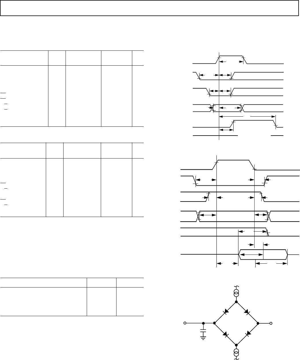
DIGITAL SPECIFICATIONS
Parameter Test Conditions Min Max Units
LOGIC INPUTS
V
IH
High Level Input Voltage +2.0 V
LOGIC
+0.5 V V
V
IL
Low Level Input Voltage –0.5 +0.8 V
I
IH
High Level Input Current (V
IN
= 5 V) V
IN
= V
LOGIC
–10 +10 µA
I
IL
Low Level Input Current (V
IN
= 0 V) V
IN
= 0 V –10 +10 µA
C
IN
Input Capacitance 10 pF
LOGIC OUTPUTS
V
OH
High Level Output Voltage I
OH
= 0.5 mA +2.4 V
V
OL
Low Level Output Voltage I
OL
= 1.6 mA +0.4 V
I
OZ
High-Z Leakage Current V
IN
= 0 to V
LOGIC
–10 +10 µA
C
OZ
High-Z Output Capacitance 10 pF
NOTES
1
f
IN
amplitude = –0.5 dB (9.44 V p-p) 10 V bipolar mode unless otherwise noted. All measurements referred to –0 dB (9.997 V p-p) input signal unless
otherwise noted.
2
Specified at worst case temperatures and supplies after one minute warm-up.
3
See Figures 12 and 13 for other input frequencies and amplitudes.
4
See Figure 11.
5
fa = 9.08 kHz, fb = 9.58 kHz with f
SAMPLE
= 100 kHz. See Definition of Specifications section and Figure 15.
All min and max specifications are guaranteed.
Specifications subject to change without notice.
–4–
REV. C
(T
MIN
to T
MAX
, with V
CC
= +15 V 6 10% or +12 V 6 5%, V
LOGIC
= +5 V 6 10%, V
EE
= –15 V 610% or
–12 V 6 5%, f
SAMPLE
= 100 kSPS, f
IN
= 10 kHz, stand-alone mode unless otherwise noted)
1
(for all grades T
MIN
to T
MAX
, with V
CC
= +15 V 6 10% or +12 V 6 5%, V
LOGIC
= +5 V 6 10%,
V
EE
= –15 V 6 10% or –12 V 6 5%)
AD1674
REV. C
–5–
(for all grades T
MIN
to T
MAX
with V
CC
= +15 V 6 10% or +12 V 6 5%,
V
LOGIC
= +5 V 610%, V
EE
= –15 V 6 10% or –12 V 6 5%; V
IL
= 0.4 V,
V
IH
= 2.4 V unless otherwise noted)
SWITCHING SPECIFICATIONS
CONVERTER START TIMING (Figure 1)
J, K, A, B, Grades T Grade
Parameter Symbol Min Typ Max Min Typ Max Units
Conversion Time
8-Bit Cycle t
C
78 78µs
12-Bit Cycle t
C
910 910µs
STS Delay from CE t
DSC
200 225 ns
CE Pulse Width t
HEC
50 50 ns
CS to CE Setup t
SSC
50 50 ns
CS Low During CE High t
HSC
50 50 ns
R/C to CE Setup t
SRC
50 50 ns
R/C Low During CE High t
HRC
50 50 ns
A
0
to CE Setup t
SAC
00ns
A
0
Valid During CE High t
HAC
50 50 ns
READ TIMING—FULL CONTROL MODE (Figure 2)
J, K, A, B, Grades T Grade
Parameter Symbol Min Typ Max Min Typ Max Units
Access Time t
DD
1
75 150 75 150 ns
Data Valid After CE Low t
HD
25
2
25
2
ns
20
3
15
4
ns
Output Float Delay t
HL
5
150 150 ns
CS to CE Setup t
SSR
50 50 ns
R/C to CE Setup t
SRR
00ns
A
0
to CE Setup t
SAR
50 50 ns
CS Valid After CE Low t
HSR
00ns
R/C High After CE Low t
HRR
00ns
A
0
Valid After CE Low t
HAR
50 50 ns
NOTES
1
t
DD
is measured with the load circuit of Figure 3 and is defined as the time
required for an output to cross 0.4 V or 2.4 V.
2
0°C to T
MAX
.
3
At –40°C.
4
At –55°C.
5
t
HL
is defined as the time required for the data lines to change 0.5 V when
loaded with the circuit of Figure 3.
All min and max specifications are guaranteed.
Specifications subject to change without notice.
Test V
CP
C
OUT
Access Time High Z to Logic Low 5 V 100 pF
Float Time Logic High to High Z 0 V 10 pF
Access Time High Z to Logic High 0 V 100 pF
Float Time Logic Low to High Z 5 V 10 pF
t
HEC
CE
STS
DB11 – DB0
A
0
CS
__
R/C
_
t
SSC
t
HSC
t
SRC
t
HRC
t
SAC
t
HAC
t
C
t
DSC
HIGH IMPEDANCE
Figure 1. Converter Start Timing
HIGH
IMPEDANCE
CE
STS
DB11 – DB0
A
0
CS
__
R/C
_
t
HSR
t
SSR
t
HRR
t
SAR
t
HAR
t
DD
t
HL
HIGH
IMP.
DATA
VALID
t
HD
t
HS
t
SSR
Figure 2. Read Timing
V
CP
D
OUT
C
OUT
I
OH
I
OL
Figure 3. Load Circuit for Bus Timing Specifications

AD1674AR-REEL

Mfr. #:
Manufacturer:
Description:
Analog to Digital Converters - ADC 12-Bit 100 kSPS Complete IC
Lifecycle:
New from this manufacturer.
Delivery:
DHL FedEx Ups TNT EMS
Payment:
T/T Paypal Visa MoneyGram Western Union