10
Electrical/Optical Characteristics 0 to 70°C; 5.25 V ≥ V
CC
≥ 4.75 V; power supply must be ltered (see Figure 1, Note 2).
Parameter Symbol Min. Typ. Max. Unit Test Condition Note
AC Responsivity 1 mm POF R
P,APF
1.7 3.9 6.5 mV/μW 650 nm Note 4
AC Responsivity 200 μm HCS R
P,HCS
4.5 7.9 11.5 mV/μW
RMS Output Noise V
NO
0.46 0.69 mV
RMS
Note 5
Equivalent Optical Noise Input P
N,RMS
- 39 -36 dBm Note 5
Power, RMS - 1 mm POF
Equivalent Optical Noise Input P
N,RMS
-42 -40 dBm Note 5
Power, RMS - 200 μm HCS
Peak Input Optical Power - P
R
-5.8 dBm 5 ns PWD Note 6
1 mm POF
-6.4 dBm 2 ns PWD
Peak Input Optical Power - P
R
-8.8 dBm 5 ns PWD Note 6
200 μm HCS
-9.4 dBm 2 ns PWD
Output Impedance Z
O
30 Ω 50 MHz Note 4
DC Output Voltage V
O
0.8 1.8 2.6 V P
R
= 0 μW
Supply Current I
CC
9 15 mA
Electrical Bandwidth BW
E
65 125 MHz -3 dB electrical
Bandwidth * Rise Time 0.41 Hz * s
Electrical Rise Time, 10-90% t
r
3.3 6.3 ns P
R
= -10 dBm
peak
Electrical Fall Time, 90-10% t
f
3.3 6.3 ns P
R
= -10 dBm
peak
Pulse Width Distortion PWD 0.4 1.0 ns P
R
= -10 dBm Note 7
peak
Overshoot 4 % P
R
= -10 dBm Note 8
peak
Notes:
1. 1.6 mm below seating plane.
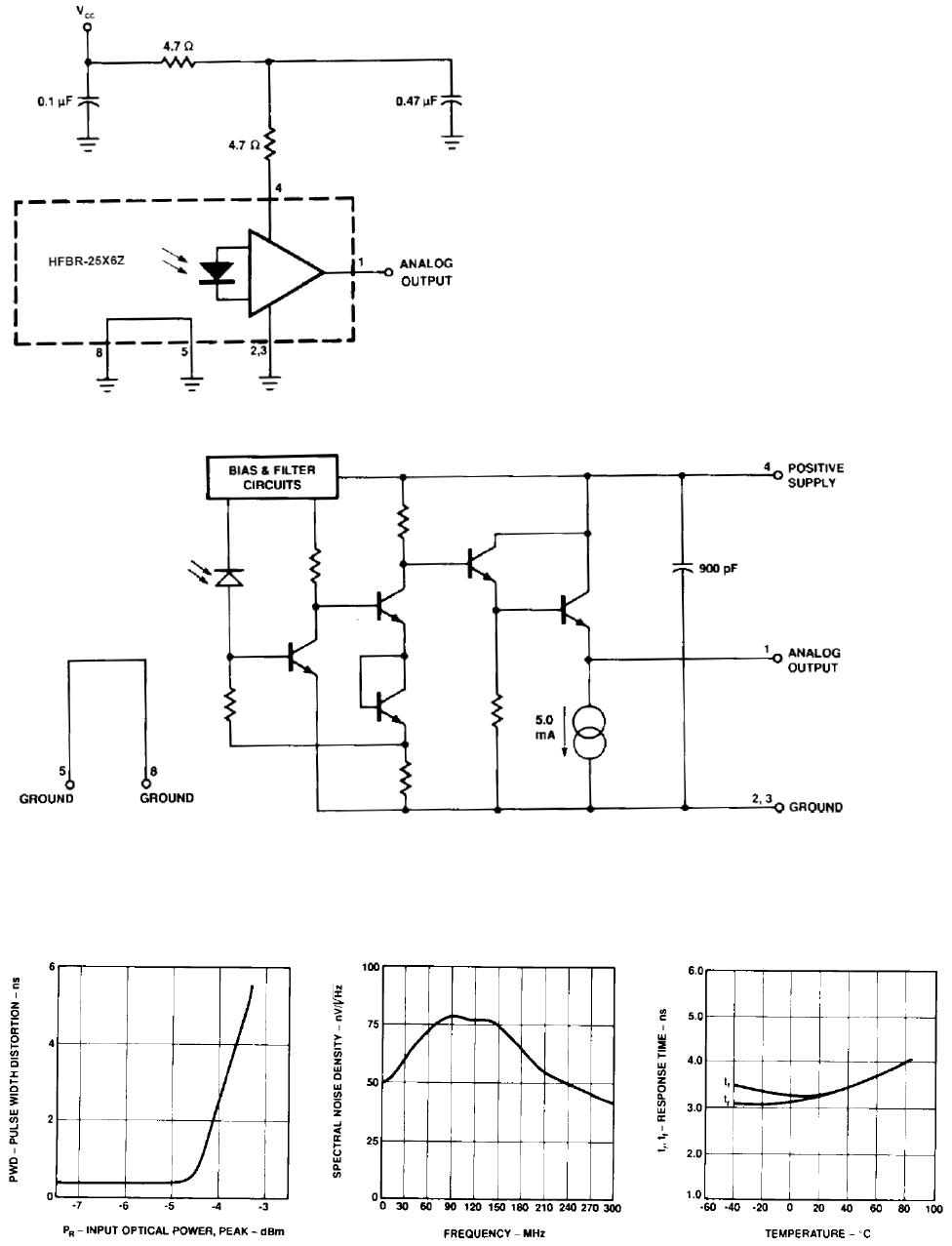
2. The signal output is an emitter follower, which does not reject noise in the power supply. The power supply must be ltered as in Figure 1.
3. Typical data are at 25°C and V
CC
= +5 Vdc.
4. Pin 1 should be ac coupled to a load ≥ 510 Ω with load capacitance less than 5 pF.
5. Measured with a 3 pole Bessel lter with a 75 MHz, -3dB bandwidth.
6. The maximum Peak Input Optical Power is the level at which the Pulse Width Distortion is guaranteed to be less than the PWD listed under
Test Condition. P
R,Max
is given for PWD = 5 ns for designing links at ≤ 50 MBd operation, and also for PWD = 2 ns for designing links up to 125
MBd (for both POF and HCS input conditions).
7. 10 ns pulse width, 50% duty cycle, at the 50% amplitude point of the waveform.
8. Percent overshoot is de ned at:
(V
PK
- V
100%
)
–––––––––––– 100%
V
100%
9. Pins 5 and 8 are primarily for mounting and retaining purposes, but are electrically connected. It is recommended that these pins be con-
nected to ground to reduce coupling of electrical noise.
10. If there is no input optical power to the receiver (no transmitted signal) electrical noise can result in false triggering of the receiver. In typical
applications, data encoding and error detection prevent random triggering from being interpreted as valid data. Refer to Application Note 1066
for design guidelines.
11. Moisture sensitivity level (MSL) is 4