10
LTC1067/LTC1067-50
ODES OF OPERATIO
U
W
The parallel combination of R5 and R6 should be kept
below 5k.
Please refer to the Operating Limits paragraph under Appli-
cations Information for a guide to the use of capacitor C
C
.
Mode 3
In Mode 3, the ratio of the external clock frequency to the
center frequency of each 2nd order section can be ad-
justed above or below the part’s nominal ratio. Figure 5
illustrates Mode 3, the classical state variable configura-
tion, providing highpass, bandpass and lowpass 2nd
order filter functions. Mode 3 is slower than Mode 1. Mode
3 can be used to make high order all-pole bandpass,
lowpass and highpass filters.
Please refer to the Operating Limits paragraph under Appli-
cations Information for a guide to the use of capacitor C
C
.
Mode 2
Mode 2 is a combination of Mode 1 and Mode 3, shown in
Figure 6. With Mode 2, the clock-to-center frequency ratio,
f
CLK
/f
O
, is always less than the part’s nominal ratio. The
advantage of Mode 2 is that it provides less sensitivity to
resistor tolerances than does Mode 3. Mode 2 has a
highpass-notch output where the notch frequency
depends solely on the clock frequency and is therefore
less than the center frequency, f
O
.
Please refer to the Operating Limits paragraph under Appli-
cations Information for a guide to the use of capacitor C
C
.
+
Σ
AGND
R1
HP
BP
LP
V
IN
1067 F05
+
S
R2
R3
C
C
R4
f
O
=
f
CLK
RATIO
H
OHP
= – ; H
OBP
= – ;
NOTE: RATIO = 100 FOR LTC1067
= 50 FOR LTC1067-50
R2
R1
R3
R1
R4
R1
H
OLP
= –
R3
R2
R2
R4
R3
(RATIO)(0.32)(R4)
( )
1
1 –
R3
(RATIO)(0.32)(R4)
( )
1
1 –
( )
R2
R4
; Q = 1.005
Figure 5. Mode 3, 2nd Order Section Providing
Highpass, Bandpass and Lowpass Outputs
Figure 6. Mode 2, 2nd Order Filter Providing Highpass
Notch, Bandpass and Lowpass Outputs
+
Σ
AGND
R1
N
BP
LP
V
IN
1067 F04
+
S
R2
R3
C
C
R5R6
f
O
= ; f
n
= f
O
Q = ; H
ON
= – ; H
OBP
= –
H
OLP
= –
R2
R1
R3
R1
R3
R2
f
CLK
RATIO
R6
(R6 + R5)
R2
R1
R6 + R5
R6
R6
(R6 + R5)
()
NOTE: RATIO = 100 FOR LTC1067
= 50 FOR LTC1067-50
Figure 4. Mode 1b, 2nd Order Filter Providing Notch,
Bandpass and Lowpass Outputs
+
Σ
AGND
R1
HPN
BP
LP
V
IN
1067 F06
+
S
R2
R3
C
C
R4
f
O
= ; f
n
=
f
CLK
RATIO
R2
R4
1 +
f
CLK
RATIO
Q = 1.005
R3
R2
( )
R2
R4
1 +
H
OHPN
= – (AC GAIN, f >> f
O
); H
OHPN
= –
R2
R1
R2
R1
R2
R1
1
R2
R4
1 +
( )
(DC GAIN)
H
OBP
= –
R3
R1
; H
OLP
= –
NOTE: RATIO = 100 FOR LTC1067
= 50 FOR LTC1067-50
R3
(RATIO)(0.32)(R4)
( )
1
1 –
R3
(RATIO)(0.32)(R4)
( )
1
1 –
1
R2
R4
1 +
( )
11
LTC1067/LTC1067-50
ODES OF OPERATIO
U
W
Mode 3a
This is an extension of Mode 3 where the highpass and
lowpass outputs are summed through two external resis-
tors, R
H
and R
L
, to create a notch (see Figure 7). Mode 3a
is more versatile than Mode 2 because the notch fre-
quency can be higher or lower than the center frequency
of the 2nd order section. The external op amp of Figure 7
is not always required. When cascading the sections of the
LTC1067, the highpass and lowpass outputs can be
summed directly into the inverting input of the next
section.
Please refer to the Operating Limits paragraph under Appli-
cations Information for a guide to the use of capacitor C
C
.
Figure 7. Mode 3a, 2nd Order Filter Providing a Highpass Notch or Lowpass Notch Output
Mode 2n
This mode extends the circuit topology of Mode 3a to
Mode 2 (Figure 8) where the highpass-notch and lowpass
outputs are summed through two external resistors, R
H
and R
L
, to create a lowpass output with a notch higher in
frequency than the notch in Mode 2. This mode, shown in
Figure 8, is most useful in lowpass elliptic designs. When
cascading the sections of the LTC1067, the highpass-
notch and lowpass outputs can be summed directly into
the inverting input of the next section.
Please refer to the Operating Limits paragraph under Appli-
cations Information for a guide to the use of capacitor C
C
.
Figure 8. Mode 2n, 2nd Order Filter Providing a Lowpass Notch Output
+
Σ
AGND
R1
HP
BP
LP
V
IN
1067 F07
+
S
R2
R3
R4
C
C
+
EXTERNAL OP AMP OR INPUT OP
AMP OF THE LTC1067, SIDES A OR B
HIGHPASS
OR LOWPASS
NOTCH OUTPUT
R
G
R
L
R
H
R2
R1
( )
R
G
R
H
()
f
O
=
;
f
n
=
H
OHPn
(f = ) = ; H
OLPn
(f = 0) =
f
CLK
RATIO
f
CLK
RATIO
R
H
R
L
R2
R4
Q = 1.005
R3
R2
R2
R4
( )
R4
R1
( )
R
G
R
L
()
NOTE: RATIO = 100 FOR LTC1067
= 50 FOR LTC1067-50
R3
(RATIO)(0.32)(R4)
( )
1
1 –
+
Σ
AGND
R1
HP
BP
LP
V
IN
1067 F08
+
S
R2
R3
R4
C
C
+
EXTERNAL OP AMP OR INPUT OP AMP
OF THE LTC1067, SIDES A OR B
LOWPASS
NOTCH
OUTPUT
R
G
R
L
R
H
f
O
=
f
n
=
H
OLPn
(f = 0)= +
f
CLK
RATIO
f
CLK
RATIO
R
H
R
L
1 +
R2
R1
R
G
R
L
R
G
R
H
()
1
R2
R4
1 +
( )
( )
R2
R4
1 +
Q = 1.005
R3
R2
( )
R2
R4
1 +
NOTE: RATIO = 100 FOR LTC1067
= 50 FOR LTC1067-50
R3
(RATIO)(0.32)(R4)
( )
1
1 –
12
LTC1067/LTC1067-50
APPLICATIONS INFORMATION
WUU
U
A switched-capacitor integrator generally exhibits a higher
input offset than a discrete RC integrator. The larger offset
is mainly due to the charge injection from the CMOS
switches into the integrated capacitor. The integrator’s op
amp offset, typically a couple of millivolts, also adds to the
overall offset value. Figure 9 shows the input offsets from
a single 2nd order section. Table 2 lists the formula for the
output offset voltage for various modes and output pins.
+
HP/N BP
+
LP
V
OS2
V
OS3
1067 F09
V
OS1
INV
S
Table 2. Output DC Offsets for a Second Order Section
MODE V
OSHP/N
V
OSBP
V
OSLP
1V
OS1
[1 + (R2/R3) + (R2/R1)] – (V
OS3
)(R2/R3) V
OS3
V
OSHP/N
– V
OS2
1b V
OS1
[1 + (R2/R3) + (R2/R1)] – (V
OS3
)(R2/R3) V
OS3
(V
OSHP/N
– V
OS2
)[1 + (R5/R6)]
2V
OS1
[1 + (R2/R3) + (R2/R1) + (R2/R4) – (V
OS3
)V
OS3
V
OSHP/N
– V
OS2
(R2/R3)](R4/R2 + R4) + (V
OS2
)(R2/R2 + R4)
3V
OS2
V
OS3
V
OS1
[1 + (R4/R1) + (R4/R2) + (R4/R3)] – (V
OS2
)
(R4/R2) – (V
OS3
)(R4/R3)
limits defined by the Typical Performance Characteristics
graphs, passband gain variations of 2dB or more should be
expected.
Clock Feedthrough
Clock feedthrough is defined as the RMS value of the clock
frequency and its harmonics that are present at the filter’s
output pins. The clock feedthrough is tested with the
filter’s input grounded and depends on PC board layout
and on the value of the power supplies. With proper layout
techniques, the typical values of clock feedthrough are
listed under Electrical Characteristics.
Any parasitic switching transients during the rising and
falling edges of the incoming clock are not part of the clock
feedthrough specifications. Switching transients have fre-
quency contents much higher than the applied clock; their
amplitude strongly depends on scope probing techniques
as well as grounding and power supply bypassing. The
clock feedthrough, can be greatly reduced by adding a
simple RC lowpass network at the final filter output. This
RC will completely eliminate any switching transients.
Wideband Noise
The wideband noise of the filter is the total RMS value of
the device’s noise spectral density and is used to deter-
mine the operating signal-to-noise ratio. Most of its fre-
quency contents lie within the filter passband and cannot
be reduced with post filtering. For a notch filter the noise
of the filter is centered at the notch frequency.
The total wideband noise (µV
RMS
) is nearly independent of
the value of the clock. The clock feedthrough specifica-
tions are not part of the wideband noise.
For a specific filter design, the total noise depends on the
Q of each section and the cascade sequence.
Operating Limits
The Maximum Q vs Frequency (f
O
) graphs, under Typical
Performance Characteristics, define an upper limit of
operating Q for each LTC1067 (or LTC1067-50) 2nd order
section. These graphs indicate the power supply, f
O
and Q
value conditions under which a filter implemented with an
LTC1067 will remain stable when operated at tempera-
tures of 70°C or less. For a 2nd order section, a bandpass
gain error of 3dB or less is arbitrarily defined as a condition
for stability.
When the passband gain error begins to exceed 1dB, the use
of capacitor C
C
will reduce the gain error (capacitor C
C
is
connected from the lowpass node to the inverting node of a
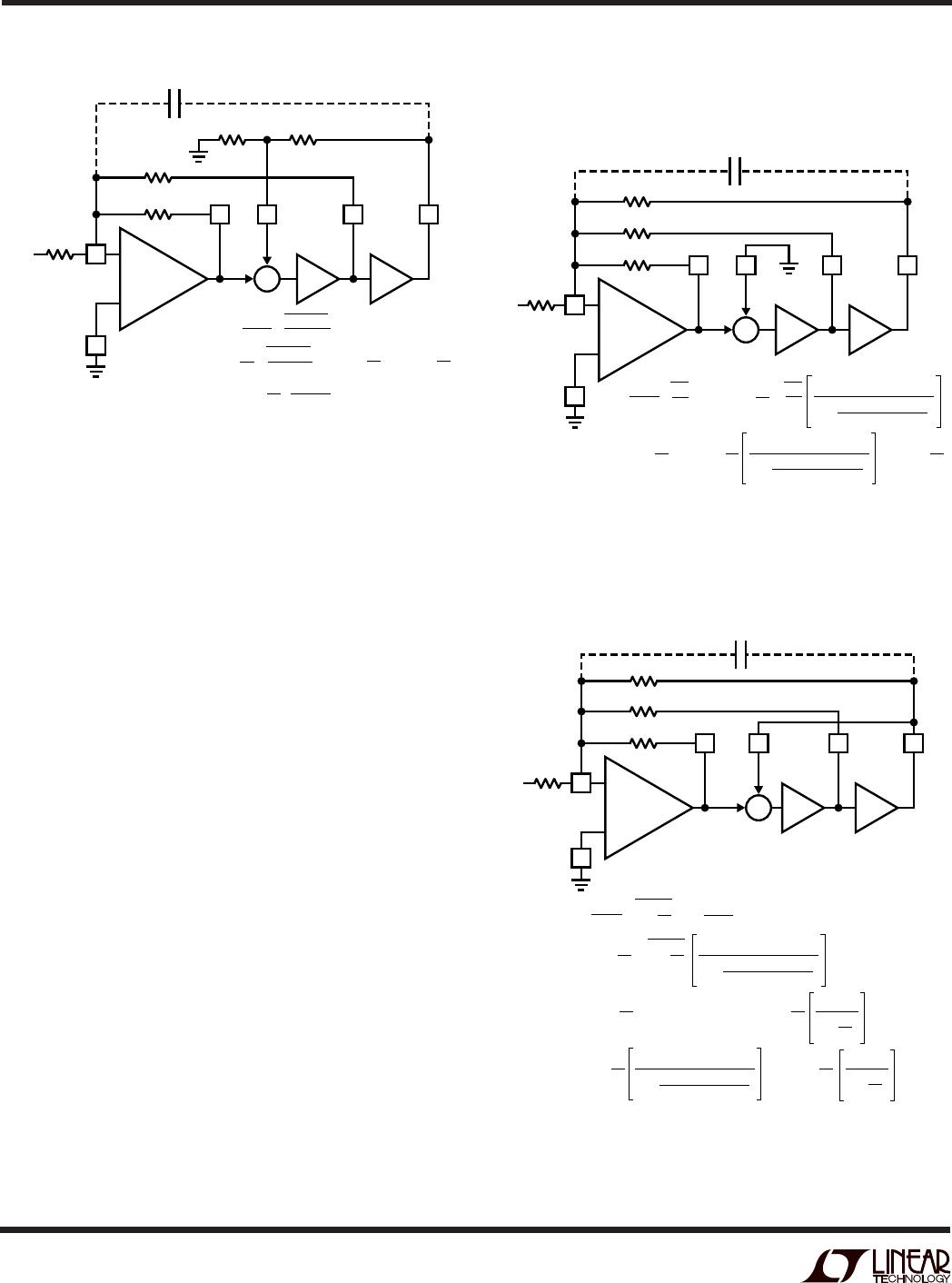
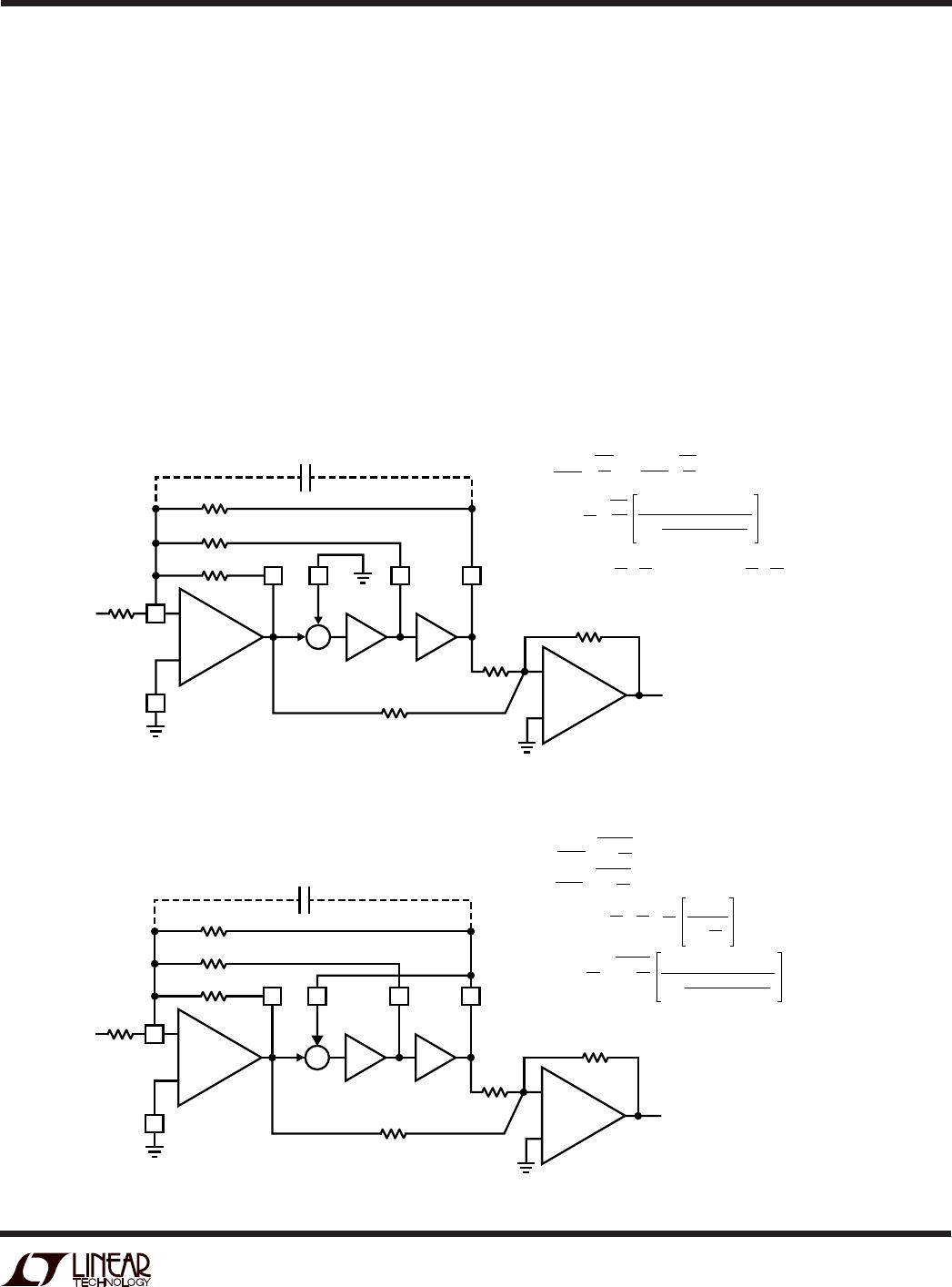
2nd order section). Please refer to Figures 3 through 8. The
value of C
C
can be best determined experimentally, and as a
guide it should be about 5pF for each 1dB of gain error and
not to exceed 15pF. When operating the LTC1067 near the
Figure 9. Block Diagram of a 2nd Order Section
Showing the Input Offsets

LTC1067-50CGN#TRPBF

Mfr. #:
Manufacturer:
Analog Devices Inc.
Description:
Active Filter R-to-R L/Noise Dual Filter Bldg Block
Lifecycle:
New from this manufacturer.
Delivery:
DHL FedEx Ups TNT EMS
Payment:
T/T Paypal Visa MoneyGram Western Union