13
LTC1067/LTC1067-50
Aliasing
Aliasing is an inherent phenomenon of switched-capacitor
filters and occurs when the frequency of the input signals
that produce the strongest aliased components have a
frequency, f
IN
, such as (f
SAMPLING
– f
IN
) that falls into the
filter’s passband. For both the LTC1067 and the
LTC1067-50, the sampling frequency is twice f
CLK
. If the
input signal spectrum is not band limited, aliasing may
occur.
Output Loading
The op amps on the LTC1067/LTC1067-50 have a rail-to-
rail output stage. The output loading issues can be divided
into resistive loading effects and capacitive loading ef-
fects.
Resistive loading effects the maximum output signal swing.
This effect is shown in the typical performance curves.
Note that the load on the output must include both the
feedback resistor and any external load resistor. For
example, consider the following situation: the part is
running on split power supplies, the section is configured
in Mode 3, the R4 resistor is 20k and an external 20k load
is connected from the LP node to ground. The load on the
LP output is 20k in parallel with 20k, or 10k. All testing on
the LTC1067/LTC1067-50 is done with a 10k load. For the
best results, the load resistance on all output pins should
be at least 10k.
Capacitive loading reduces the stability of the op amps.
The signal at the output of a switched-capacitor filter is
composed of a series of very small steps. The op amp
must respond to a step and fully settle before the next step.
As the stability of the op amp is decreased, the output step
response has increased ringing and a much longer settling
time. This longer settling time drastically lowers the maxi-
mum usable clock speed and introduces errors. If the
capacitive loading is sufficiently high, the stability will be
decreased to the point of oscillation at the output.
The LTC1067/LTC1067-50 are sensitive to capacitive load-
ing. Capacitive loading should be kept below 20pF. Good,
tight layout techniques should be maintained at all times.
These parts should not drive long traces and never drive
a long coaxial cable.
When probing the LTC1067 or
APPLICATIONS INFORMATION
WUU
U
LTC1067-50, always use a 10
×
probe. Never use a 1
×
probe.
A standard 10× probe has a capacitance of 10pF to
15pF while a 1× probe’s capacitance can be as high as
150pF. The 1× probe will probably cause oscillation.
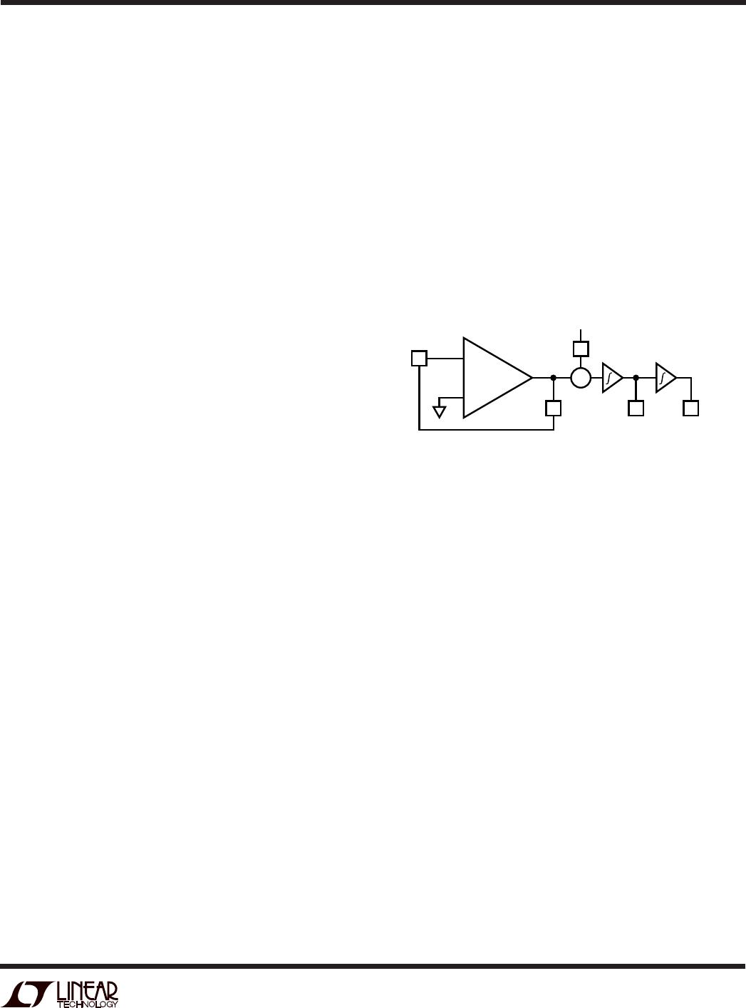
What to Do with an Unused Section
If the LTC1067 or LTC1067-50 is used as a single 2nd
order filter, the other 2nd order section is not used. Do not
leave this section unconnected. If the section is uncon-
nected, inputs and outputs are left to float to undetermined
levels and oscillation may occur. The unused section
should be connected as shown in Figure 10.
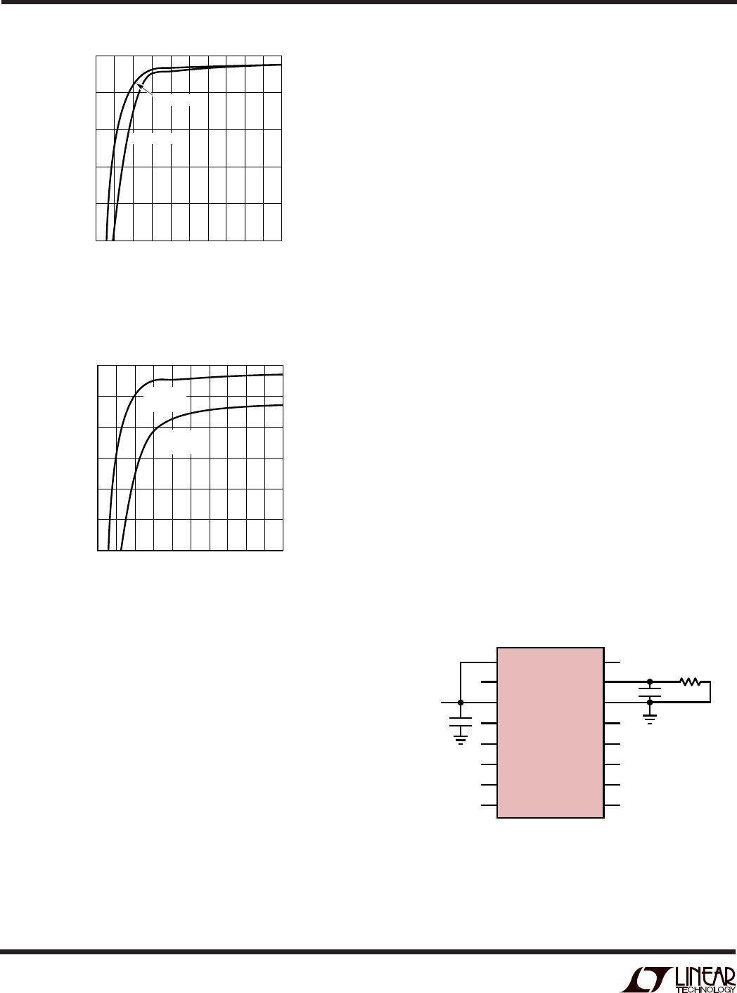
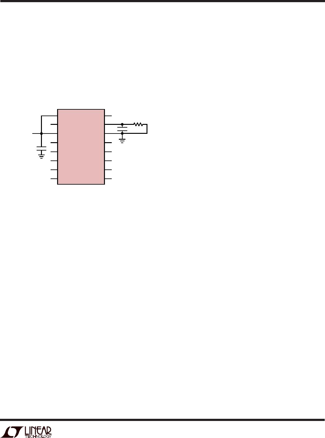
Output Voltage Swing on a Single Supply Voltage
The typical performance curves show the output voltage
swing limitations. The curves show the output signal
swing, in volts peak-to-peak, versus the output load resis-
tance. The peak-to-peak swing is limited by the following
three considerations: the op amp’s output swings closer
to the negative supply than the positive supply, the AGND
pin is biased at the midpoint of the supplies and all
operating modes are inverting.
The op amps in the LTC1067/LTC1067-50 swing closer to
the negative supply rail than the positive supply rail. The
positive output voltage swing for single supply operation
is shown in Figures 11 and 12. The negative output voltage
swing is about 15mV for the LTC1067 and 10mV for the
LTC1067-50. The negative output voltage swing is nearly
independent of load resistance since the load in this case
is connected to the V
supply rail.
For single supply applications, the on-chip resistor divider
sets the voltage at the AGND pin to the midpoint of the V
+
and V
potentials. The AGND voltage is the reference for
all internal op amps. If the input to the filter is at the V
rail,
+
V
+
1067 F10
INV
HP
BP LP
Figure 10. Connections for an Unused Section
14
LTC1067/LTC1067-50
APPLICATIONS INFORMATION
WUU
U
Many applications are more concerned with the negative
output swing than the positive output swing. Interfacing to
an ADC running on a single 5V supply with a 4.096
reference voltage is a standard example. The LTC1067 or
LTC1067-50 will easily reach the 4.096V level for a full-
scale reading. The issue is how close does the output go
to ground. The further the output is from ground, the more
codes that are essentially lost. The previous example
demonstrated that the lowest output voltage would be
about 250mV, although, as is shown below, 15mV is
achievable.
To achieve a lower negative output swing voltage, the
AGND voltage must be adjusted down below the midpoint.
The AGND voltage is determined by two equal, on-chip
resistors. These resistors are typically 15k each. While the
ratio of these two resistors is tightly matched, the absolute
value of the resistors is not tightly controlled. Adjusting
the AGND voltage by simply adding an external resistor
can be done, but caution must be exercised.
In Figure 13, a resistor is used to adjust the AGND voltage
for use with a 5V powered ADC with a full-scale input of
4.096V. The resistor value was chosen carefully to assure
that a 4.096V input signal to the filter yields a full-scale
reading from the ADC and a 0V input signal gives the
lowest possible value (15mV for the LTC1067 and 10mV
for the LTC1067-50). The circuit works well over tempera-
ture and part variations. For this application, the 5V supply
must be above 4.75V.
LOAD RESISTANCE (k TO V
)
POSITIVE OUTPUT VOLTAGE SWING (V)
5.0
4.5
4.0
3.5
3.0
2.5
1067 F11
100 2 4 6 8 12 14 16 18 20
LTC1067-50
LTC1067
Figure 11. LTC1067/LTC1067-50 Positive Output Voltage
Swing vs Load Resistance, 5V Supply
the output of the first section is near the positive rail
(operating modes invert the signal). The output of the first
stage will saturate at about 250mV (typical for 5V supply)
from positive supply. The output from the second stage
will be 250mV from the negative supply rail (assuming
inversion again) even though the op amp’s output is
capable of swinging to within 15mV.
The positive output voltage swing being less than the
negative swing, coupled with the AGND potential set at the
midpoint of the supplies and inverting of the signal, yields
the following equation for peak-to-peak output swing:
V
P-P
Swing = (V
+
– V
) – 2(V
+
– V
POSITIVE
SWING
)
LOAD RESISTANCE (k TO V
)
POSITIVE OUTPUT VOLTAGE SWING (V)
3.3
3.0
2.7
2.4
2.1
1.8
1.5
1067 F12
100 2 4 6 8 12 14 16 18 20
LTC1067-50
V
S
= 3V
LTC1067
V
S
= 3.3V
Figure 12. LTC1067/LTC1067-50 Positive Output Voltage
Swing vs Load Resistance, 3.3V/3V Supplies
0.1µF
1067 F13
64.9k
1%
LTC1067
LTC1067-50
16
15
14
13
12
11
10
9
1
2
3
4
5
6
7
8
V
+
NC
V
+
SA
LPA
BPA
HPA/NA
INV A
CLK
AGND
V
SB
LPB
BPB
HPB/NB
INV B
5V
(4.75V
MIN
)
1µF
Figure 13. Power and AGND Connections for
5V ADC with 4.096V Full Scale
15
LTC1067/LTC1067-50
APPLICATIONS INFORMATION
WUU
U
Figure 14 illustrates how a resistor adjusts the AGND
voltage for use with a 3V/3.3V powered ADC with a full-
scale input of 2.048V. As in the previous circuit, the
resistor value was chosen carefully to assure that a 2.048V
input signal to the filter yields a full-scale reading from the
ADC and a 0V input signal gives the lowest possible value.
For this application, the power supply must be above 2.7V
for an LTC1067-50 filter and above 3V for an LTC1067
filter.
Figure 14. Power and AGND Connections for
3V/3.3V ADC with 2.048V Full Scale
0.1µF
1067 F14
33.2k
1%
LTC1067
LTC1067-50
16
15
14
13
12
11
10
9
1
2
3
4
5
6
7
8
V
+
NC
V
+
SA
LPA
BPA
HPA/NA
INV A
CLK
AGND
V
SB
LPB
BPB
HPB/NB
INV B
3V TO 3.6V
(LTC1067)
2.7V TO 3.6V
(LTC1067-50)
1µF
Semi-Custom Filter Program
Linear Technology has in place a program to deliver fully
integrated filters, custom designed for any specified appli-
cation. These semi-custom filters are based on an existing
universal filter product with integrated, on-chip resistors.
The final filter is then tested to the exact parameters
defined for the application. The final result is a fully
integrated, accurately tested solution in a smaller pack-
age. For the LTC1067 or LTC1067-50 parts, a semi-
custom filter comes in the SO-8 package and requires only
a clock and a decoupling capacitor. For more details on the
semi-custom filter program, contact Linear Technology’s
marketing department.
Demonstration Board
There is a demonstration board available for the LTC1067/
LTC1067-50. Demonstration board 150A has the LTC1067
part installed and the board 150B has the LTC1067-50
installed. The schematic for the board is shown in Figure
15 and the assembly drawing is shown in Figure 16. To
obtain a demonstration board, call your local representa-
tive or Linear Technology’s marketing department.
The demonstration board has all integrated circuits, con-
nectors and decoupling capacitors installed. The board is
ready to be configured with the appropriate resistors and
jumper connections.
There are two sets of power supply connections. One is for
the LTC1067/LTC1067-50 and the other is for the buffer-
ing op amp on the board. Having separate connections
gives the board the most flexibility. The two sets of
supplies can be connected together if a common supply is
desired.
When configuring the board for split supply operation, a
jumper wire must be installed in the JPAGND position.
This connects the AGND pin of the device to the ground
plane of the board. The JPVNEG jumper must be left open.
The power supply is then connected to V
+
, V
and GND
turrets (all of the GND turrets on the board are the same).
For single supply operation, insert a wire in the JPVNEG
jumper and leave the JPAGND jumper open. This connects
the V
pin to the board’s ground plane. The JPAGND
jumper must be left open so that the on-chip resistor
network can set the AGND potential at the midpoint of the
supply. Connect the power supply to V
+
and any GND
turret. The V
turret can be left open or shorted to the
adjacent GND turret. If the buffering op amp is run on the
same single voltage supply, the VOA
+
turret and the V
+
turrets must be connected together and the VOA
turret
must be shorted to the adjacent GND turret.
The J1 BNC connector is the clock input. There is a 200
series resistor connected between the connector and the
CLK pin of the part. This resistor, coupled with the CLK
pin’s input capacitance, slows down the rise and fall times
of the clock signal and decreases high frequency coupling.
The clock input is not terminated to 50 or 75. An
external terminator should be used.
Jumpers JP51 and JP61 are connected in parallel with
R51 and R61 respectively. Jumper JP51 connects the LPA
pin of the part with the SA pin. This can be used for
operating modes 1 or 2. Alternatively, a 0 resistor in the
R51 position fulfills the same requirement. The JP61
jumper connects the SA pin of the part to the AGND pin.

LTC1067-50CGN#TRPBF

Mfr. #:
Manufacturer:
Analog Devices Inc.
Description:
Active Filter R-to-R L/Noise Dual Filter Bldg Block
Lifecycle:
New from this manufacturer.
Delivery:
DHL FedEx Ups TNT EMS
Payment:
T/T Paypal Visa MoneyGram Western Union