7
LTC1067/LTC1067-50
PIN FUNCTIONS
UUU
V
+
, V
(Pins 1, 3,14): The V
+
(Pins 1, 3) and the V
(Pin
14) should each be bypassed with a 0.1µF capacitor to an
adequate analog ground. The filter’s power supplies should
be isolated from other digital or high voltage analog
supplies. A low noise linear supply is recommended.
Using a switching power supply will lower the signal-to-
TYPICAL PERFORMANCE CHARACTERISTICS
U
W
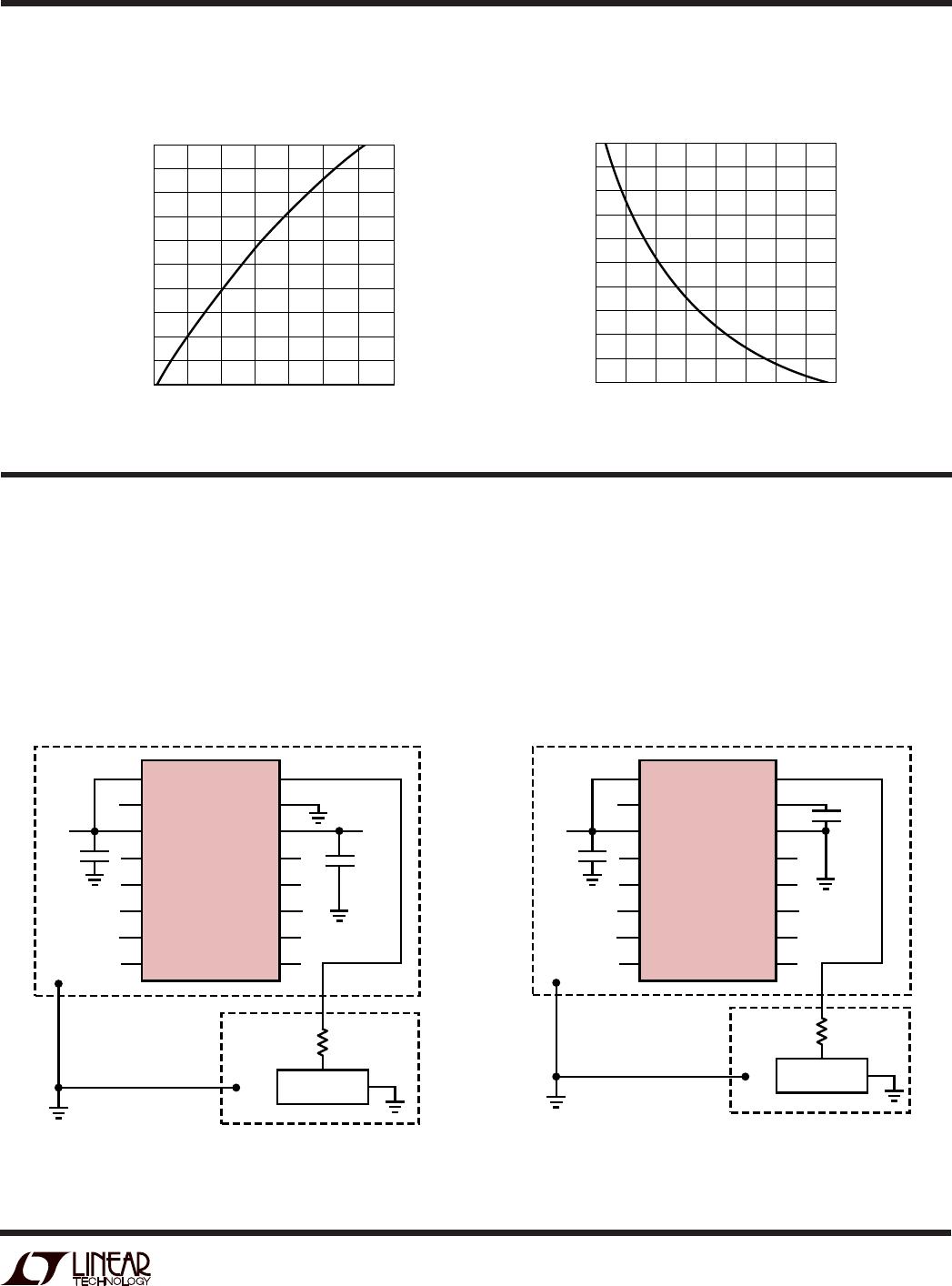
LTC1067/LTC1067-50 Mode 1B
Noise Increase vs R5/R6 Ratio
LTC1067/LTC1067-50 Mode 3
Noise Increase vs R2/R4 Ratio
R2/R4 RATIO
0.2
2.0
1.9
1.8
1.7
1.6
1.5
1.4
1.3
1.2
1.1
1.0
0.5 0.7
1067 G26
0.3 0.4
0.6 0.8 0.9 1.0
RELATIVE NOISE INCREASE
(REFERENCE NOISE WHEN R2/R4 = 1)
noise ratio of the filter. The supply’s power-up slew rate
should be less than 1V/µs. When V
+
is applied before V
, and
V
is allowed to go above ground, a diode should clamp V
to prevent latch-up. Figures 1 and 2 show typical connec-
tions for dual and single supply operation.
0.1µF
1067 F01
200
LTC1067
LTC1067-50
CLOCK
SOURCE
16
15
14
13
12
11
10
9
1
2
3
4
5
6
7
8
STAR
SYSTEM
GROUND
DIGITAL
GROUND
PLANE
V
+
NC
V
+
SA
LPA
BPA
HPA/NA
INV A
CLK
AGND
V
SB
LPB
BPB
HPB/NB
INV B
V
+
V
0.1µF
Figure 1. Dual Supply Ground Plane Connections
Figure 2. Single Supply Ground Plane Connections
0.1µF
106 7 F02
200
LTC1067
LTC1067-50
CLOCK
SOURCE
16
15
14
13
12
11
10
9
1
2
3
4
5
6
7
8
STAR
SYSTEM
GROUND
DIGITAL
GROUND
PLANE
V
+
NC
V
+
SA
LPA
BPA
HPA/NA
INV A
CLK
AGND
V
SB
LPB
BPB
HPB/NB
INV B
V
+
1µF
FOR MODE 3, THE SA AND SB SUMMING NODE PINS
ARE TIED TO THE AGND PIN
R5/R6 RATIO
0
2.0
1.9
1.8
1.7
1.6
1.5
1.4
1.3
1.2
1.1
1.0
1.5 2.5
1067 G25
0.5 1.0
2.0 3.0 3.5
RELATIVE NOISE INCREASE
(REFERENCE NOISE WHEN R5/R6 = 0.02)
8
LTC1067/LTC1067-50
PIN FUNCTIONS
UUU
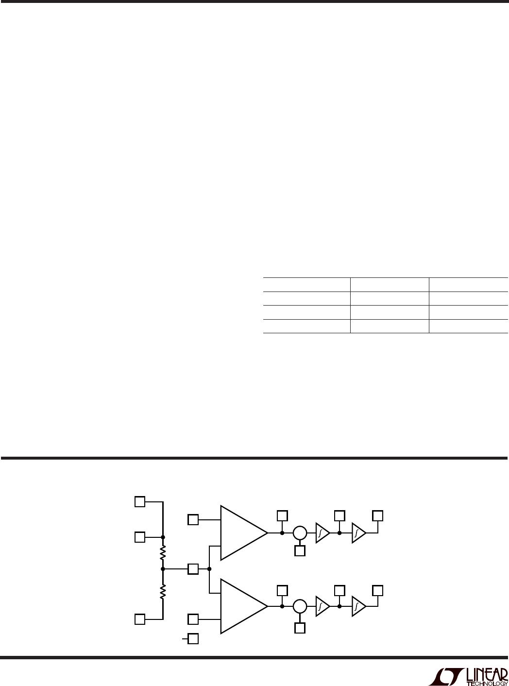
SA, SB (Pins 4, 13): Summing Inputs. The summing pins’
connection, along with the other resistor connections,
determine the circuit topology (mode) of each 2nd order
section. These pins should never be left floating.
LPA, BPA, HPA/NA, HPB/NB, BPB, LPB (Pins 5, 6, 7, 10,
11, 12): Output Pins. Each 2nd order section of the
LTC1067 has three outputs which typically source 33mA
and sink 2mA. Driving coaxial cable, capacitive loads or
resistive loads less than 10k will degrade the total har-
monic distortion performance of any filter design. Refer to
Output Loading in the Applications Information section for
more details. When evaluating the distortion or noise
performance of a filter, the output should be buffered with
a wideband amplifier.
INV A, INV B (Pins 8, 9): Inverting Input. These pins are
the high impedance inverting inputs of internal op amps.
They are susceptible to stray capacitance coupling to low
impedance nodes such as signal outputs and power
supply lines. Resistors that are connected from a signal
output to the inverting input pin should be located as close
to the inverting input as possible.
AGND (Pin 15): Analog Ground. The filter performance
depends on the quality of the analog signal ground. For
either dual or single supply operation, an analog ground
plane surrounding the package is recommended. The
analog ground plane should be connected to any digital
ground at a single point. For dual supply operation Pin 15
is connected to the analog ground plane. For single supply
operation Pin 15 should be bypassed to the analog ground
plane with at least a 1µF capacitor. An on-chip resistive
voltage divider sets the bias at one-half of the supply.
CLK (Pin 16): Clock Input. Any CMOS logic clock source
with a square-wave output and a 50% duty cycle (±10%)
is an adequate clock source for the device. The power
supply for the clock source should not be the filter’s power
supply. The analog ground for the filter should be con-
nected to the clock’s ground at a single point only. Table
1 shows the clock’s low and high level threshold values for
dual supply or single supply operation. Logic low level
signals must be greater than the negative supply voltage.
With a ±5V power supply, the clock levels may be either
±5V or 0V to 5V. Logic high level signals should be less
than the positive supply voltage. However, when the
positive supply voltage is either 3V or 3.3V, the clock
signal can be as high as 5.5V.
Table 1. Clock Source High and Low Threshold Levels
POWER SUPPLY HIGH LEVEL LOW LEVEL
±5V 2.2V 0.50V
Single 5V 2.2V 0.50V
Single 3V, 3.3V 2V 0.40V
Sine waves are not recommended for the clock input. The
clock signal should be routed from the right side of the IC
package to avoid coupling to any power supply lines or
input or output signal paths. A 200 resistor between the
clock source and Pin 16 will slow down the rise and fall
times of the clock to reduce charge coupling of the clock.
This will result in less clock feedthrough noise on the
output signal.
BLOCK DIAGRA
W
+
+
INV A
INV B
CLK
V
V
+
V
+
1
3
8
14
HPA/NA
BPA
LPA
SA
HPB/NB
BPB LPB
SB
AGND
15k
15k
1067 BD
+
+
15
9
16
10
13
11 12
7
4
65
9
LTC1067/LTC1067-50
ODES OF OPERATIO
U
W
Mode 1
In Mode 1, the ratio of the external clock frequency to the
center frequency of each 2nd order section is internally
fixed at the part’s nominal ratio. Figure 3 illustrates Mode
1 providing 2nd order notch, lowpass and bandpass
outputs. Mode 1 can be used to make high order Butter-
worth lowpass filters; it can also be used to make low Q
notches and for cascading 2nd order bandpass functions
tuned at the same center frequency. Mode 1 is faster than
Mode 3.
Please refer to the Operating Limits paragraph under Appli-
cations Information for a guide to the use of capacitor C
C
.
Linear Technology’s universal switched-capacitor filters
are designed with a fixed internal, nominal f
CLK
/f
O
ratio.
The LTC1067 has a 100:1 f
CLK
/f
O
ratio and the
LTC1067-50 has a 50:1 f
CLK
/f
O
ratio. Filter designs often
require the f
CLK
/f
O
ratio of each section to be different from
the nominal ratio and in most cases different from each
other. Ratios other than the nominal value are possible
with external resistors. Operating modes use external
resistors, connected in different arrangements to realize
different f
CLK
/f
O
ratios. By choosing the proper mode, the
f
CLK
/f
O
ratio can be increased or decreased from the part’s
nominal ratio.
The choice of operating mode also effects the transfer
function at the HP/N pins. The LP and BP pins always give
the lowpass and bandpass transfer functions respectively,
regardless of the mode utilized. The HP/N pins have a
different transfer function depending on the mode used.
Mode 1 yields a notch transfer function. Mode 3 yields a
highpass transfer function. Mode 2 yields a highpass-
notch transfer function (i.e., a highpass with a stopband
notch). More complex transfer functions, such as low-
pass-notch, allpass or complex zeros, are achieved by
summing two or more of the LP, BP or HP/N outputs. This
is illustrated in sections Mode 2n and Mode 3a.
Choosing the proper mode(s) for a particular application
is not trivial and involves much more than just adjusting
the f
CLK
/f
O
ratio. Listed here are six of the nearly twenty
modes available. To make the design process simpler and
quicker, Linear Technology has developed the FilterCAD
TM
for Windows
®
design software. FilterCAD is an easy-to-
use, powerful and interactive filter design program. The
designer can enter a few filter specifications and the
program produces a full schematic. FilterCAD allows the
designer to concentrate on the filter’s transfer function
and not get bogged down in the details of the design.
Alternatively, those who have experience with the Linear
Technology family of parts can control all of the details
themselves. For a complete listing of all the operating
modes, consult the appendices of the FilterCAD manual or
the Help files in FilterCAD. FilterCAD can be obtained free
of charge on the Linear Technology web site (http://
www.linear-tech.com) or you can order the FilterCAD
CD-ROM by contacting Linear Technology’s marketing
department.
FilterCAD is a trademark of Linear Technology Corporation.
Windows is a registered trademark of Microsoft Corporation.
Mode 1b
Mode 1b is derived from Mode 1. In Mode 1b (Figure 4)
two additional resistors R5 and R6 are added to lower the
amount of voltage fed back from the lowpass output into
the input of the SA (or SB) switched-capacitor summer.
This allows the filter’s clock-to-center frequency ratio to
be adjusted beyond the part’s nominal ratio. Mode 1b
maintains the speed advantages of Mode 1 and should be
considered an optimum mode for high Q designs with f
CLK
to f
CUTOFF
(or f
CENTER
) ratios greater than the part’s
nominal ratio.
Figure 3. Mode 1, 2nd Order Filter Providing Notch,
Bandpass and Lowpass Outputs
+
Σ
AGND
NOTE: RATIO = 100 FOR LTC1067
= 50 FOR LTC1067-50
R1
N
BP
LP
V
IN
1067 F03
+
S
R2
R3
C
C
f
O
= ; f
n
= f
O
Q = ; H
ON
= – ; H
OBP
= –
H
OLP
= H
ON
R2
R1
R3
R1
R3
R2
f
CLK
RATIO
LTC1067-50CGN#TRPBF

Mfr. #:
Manufacturer:
Analog Devices Inc.
Description:
Active Filter R-to-R L/Noise Dual Filter Bldg Block
Lifecycle:
New from this manufacturer.
Delivery:
DHL FedEx Ups TNT EMS
Payment:
T/T Paypal Visa MoneyGram Western Union