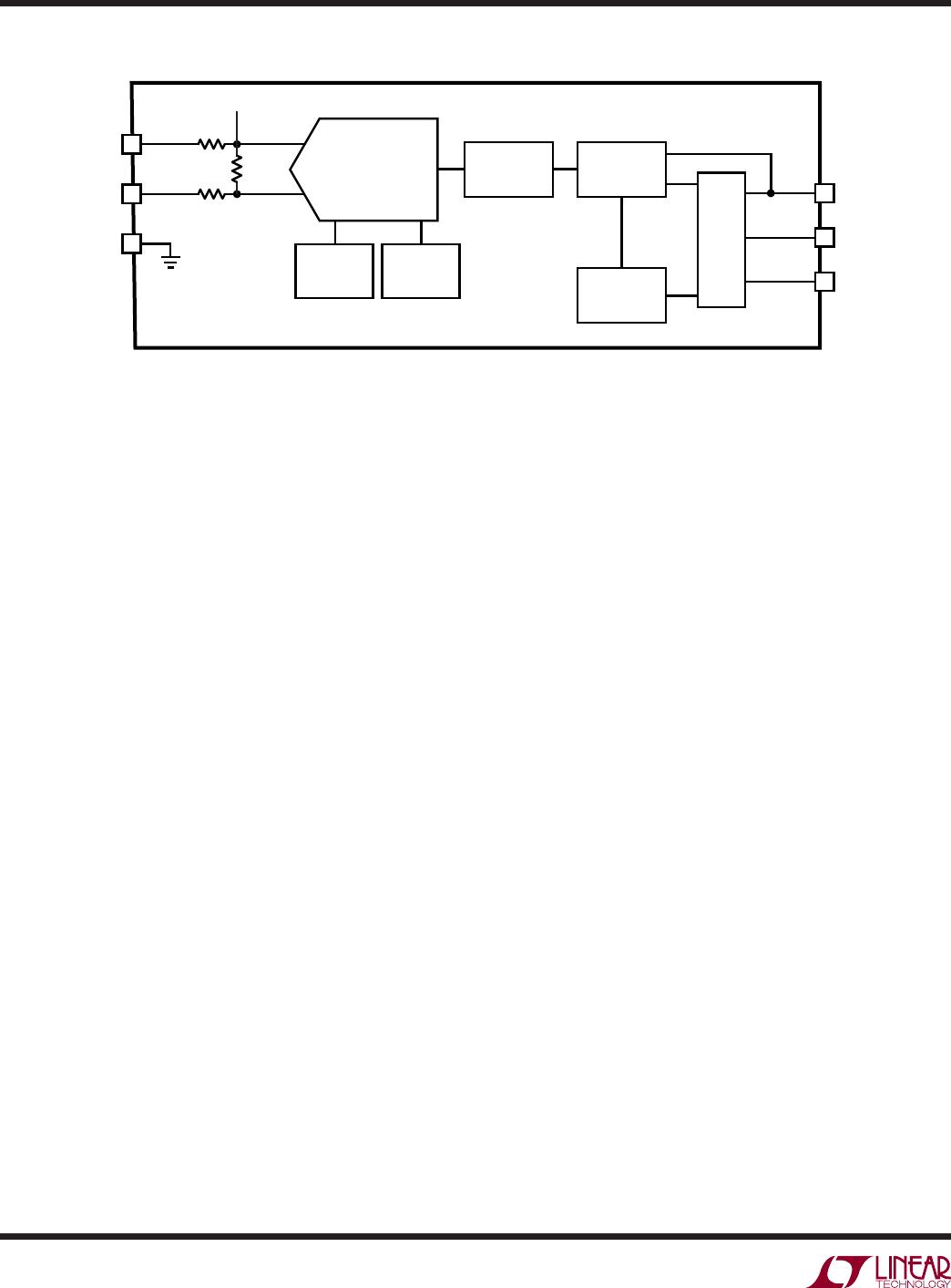
LTC2941-1
4
29411f
Typical perFormance characTerisTics
Total Charge Error
vs Sense Current
Total Charge Error
vs Supply Voltage
Total Charge Error vs Temperature
Supply Current vs Supply Voltage
Shutdown Supply Current
vs Supply Voltage
|I
SENSE
| (mA)
1
–0.50
CHARGE ERROR (%)
0
–0.25
–0.75
0.25
0.50
10 100 1000
29411 G01
–1.00
1.00
0.75
V
SENSE
+ = 2.7V
V
SENSE
+ = 4.2V
V
SENSE
+
(V)
2.5
I
SUPPLY
(µA)
80
90
100
4.0 5.0
29411 G04
70
60
3.0 3.5
4.5 5.5 6.0
50
40
T
A
= 25°C
T
A
= –40°C
T
A
= 85°C
Sense Resistor Stability
V
SENSE
+
(V)
2.5
–1.0
CHARGE ERROR (%)
–0.8
–0.4
–0.2
0
1.0
0.4
3.5
4.5
5
29411 G02
–0.6
0.6
0.8
0.2
3
4
5.5
6
|I
SENSE
| = 1A
|I
SENSE
| = 200mA
TEMPERATURE (°C)
–50
CHARGE ERROR (%)
–0.25
0
0.25
25
75
24911 G03
–0.50
–0.75
–1.00
–25 0 50
0.50
0.75
1.00
100
+50ppm/K
OPTIMUM
–50ppm/K
TEMPERATURE
COMPENSATION
TRIM DEVIATION
|I
SENSE
| = 200mA
LTC2941-1
5
29411f
pin FuncTions
SENSE
+
(Pin 1): Positive Current Sense Input and Power
Supply. Connect to the load and battery charger output.
V
SENSE
+
operating range is 2.7V to 5.5V.
GND (Pin 2): Device Ground. Connect directly to the nega-
tive battery terminal.
SCL (Pin 3): Serial Bus Clock Input.
SDA (Pin 4): Serial Bus Data Input and Output.
AL/CC (Pin 5): Alert Output or Charge Complete Input.
Configured either as an SMBus alert output or charge
complete input by control register bits B[2:1]. At power-up,
the pin defaults to alert mode conforming to the SMBus
alert response protocol. It behaves as an open-drain logic
output that pulls to GND when a value in the threshold
registers is exceeded.
When configured as a charge complete input, a high level
at CC sets the value of the accumulated charge (registers
C, D) to FFFFh. Coulomb counting starts when the input
returns to low level.
SENSE
(Pin 6): Negative Current Sense Input. Connect
SENSE
to the positive battery terminal. Current from/into
this pin must not exceed 1A in normal operation.
Exposed Pad (Pin 7): Do Not Connect. Soldering the
exposed pad to adequate electrically isolated copper area
is recommended for best thermal performance.
LTC2941-1
6
29411f
block Diagram
REF CLK
BIDIRECTIONAL
INTEGRATOR
SENSE
R
SENSE
50mΩ
INTERNAL
REFERENCE
GENERATOR
ACCUMULATED
CHARGE
REGISTER
PRESCALER
M
STATUS/
CONTROL
REGISTER
INTERNAL
OSCILLATOR
6
SENSE
+
V
SUPPLY
1
AL/CC
AL
5
GND
2
I
2
C/
SMBus
SCL
CC
SDA
29411 F02
3
4
R
BOND
12mΩ
R
BOND
12mΩ
Figure 2. Block Diagram of the LTC2941-1

LTC2941IDCB-1#TRPBF

Mfr. #:
Manufacturer:
Analog Devices / Linear Technology
Description:
Battery Management 1A I2C Bat Gas Gauge w/ Int Sense Res
Lifecycle:
New from this manufacturer.
Delivery:
DHL FedEx Ups TNT EMS
Payment:
T/T Paypal Visa MoneyGram Western Union