Data Sheet AD8428
Rev. A | Page 15 of 20
INPUT BIAS CURRENT RETURN PATH
The input bias current of the AD8428 must have a return path
to ground. When the source, such as a thermocouple, cannot
provide a current return path, one should be created, as shown
in Figure 41.
THERMOCOUPLE
+V
S
REF
–V
S
AD8428
CAPACITIVELY COUPLED
+V
S
REF
C
C
–V
S
AD8428
TRANSFORMER
+V
S
REF
–V
S
AD8428
INCORRECT
CAPACITIVELY COUPLED
+V
S
REF
C
R
R
C
–V
S
AD8428
1
f
HIGH-PASS
=
2πRC
THERMOCOUPLE
+V
S
REF
–V
S
10M
AD8428
TRANSFORMER
+V
S
REF
–V
S
AD8428
CORRECT
09731-046
Figure 41. Creating an Input Bias Current Return Path
INPUT PROTECTION
Do not allow the inputs of the AD8428 to exceed the ratings
stated in the Absolute Maximum Ratings section. If these ratings
cannot be adhered to, add protection circuitry in front of the
AD8428 to limit the maximum current into the inputs (see the
I
MAX
section).
I
MAX
The maximum current into the AD8428 inputs, I
MAX
, depends
on time and temperature. At room temperature, the device can
withstand a current of 10 mA for at least one day. This time is
cumulative over the life of the device.
Input Voltages Beyond the Rails
If voltages beyond the rails are expected, use an external resistor
in series with each input to limit current during overload condi-
tions. The limiting resistor at each input can be computed using
the following equation:
MAX
SUPPLY
IN
PROTECT
I
VV
R
Noise sensitive applications may require a lower protection
resistance. Low leakage diode clamps, such as the BAV199, can
be used at the inputs to shunt current away from the AD8428
inputs and, therefore, allow smaller protection resistor values.
To ensure that current flows primarily through the external
protection diodes, place a small value resistor, such as a 33 
resistor, between the diodes and the AD8428.
SIMPLE METHOD LOW NOISE METHOD
+V
S
AD8428
R
PROTECT
R
PROTECT
–V
S
I
V
IN+
+
V
IN–
+
+V
S
+
V
S
AD8428
R
PROTECT
33
33
R
PROTECT
–V
S
–V
S
I
V
IN+
+
V
IN–
+
+V
S
–V
S
09731-047
Figure 42. Protection for Voltages Beyond the Rails
Large Differential Input Voltage at High Gain
If large differential voltages at high gain are expected, use
an external resistor in series with each input to limit current
during overload conditions. The limiting resistor at each input
can be computed using the following equation:
×
G
MAX
DIFF
PROTECT
R
I
V
R
V1
2
1
Noise sensitive applications may require a lower protection
resistance. Low leakage diode clamps, such as the BAV199,
can be used across the AD8428 inputs to shunt current away
from the inputs and, therefore, allow smaller protection resistor
values.
AD8428
R
PROTECT
R
PROTECT
I
V
DIFF
+
09731-048
Figure 43. Protection for Large Differential Voltages
AD8428 Data Sheet
Rev. A | Page 16 of 20
RADIO FREQUENCY INTERFERENCE (RFI)
Because of its high gain and low noise properties, the AD8428
is a highly sensitive amplifier. Therefore, RF rectification can be
a problem if the AD8428 is used in applications that have strong
RF signal sources present. The problem is intensified if long leads
or PCB traces are required to connect the amplifier to the signal
source. The disturbance can appear as a dc offset voltage or as a
train of pulses.
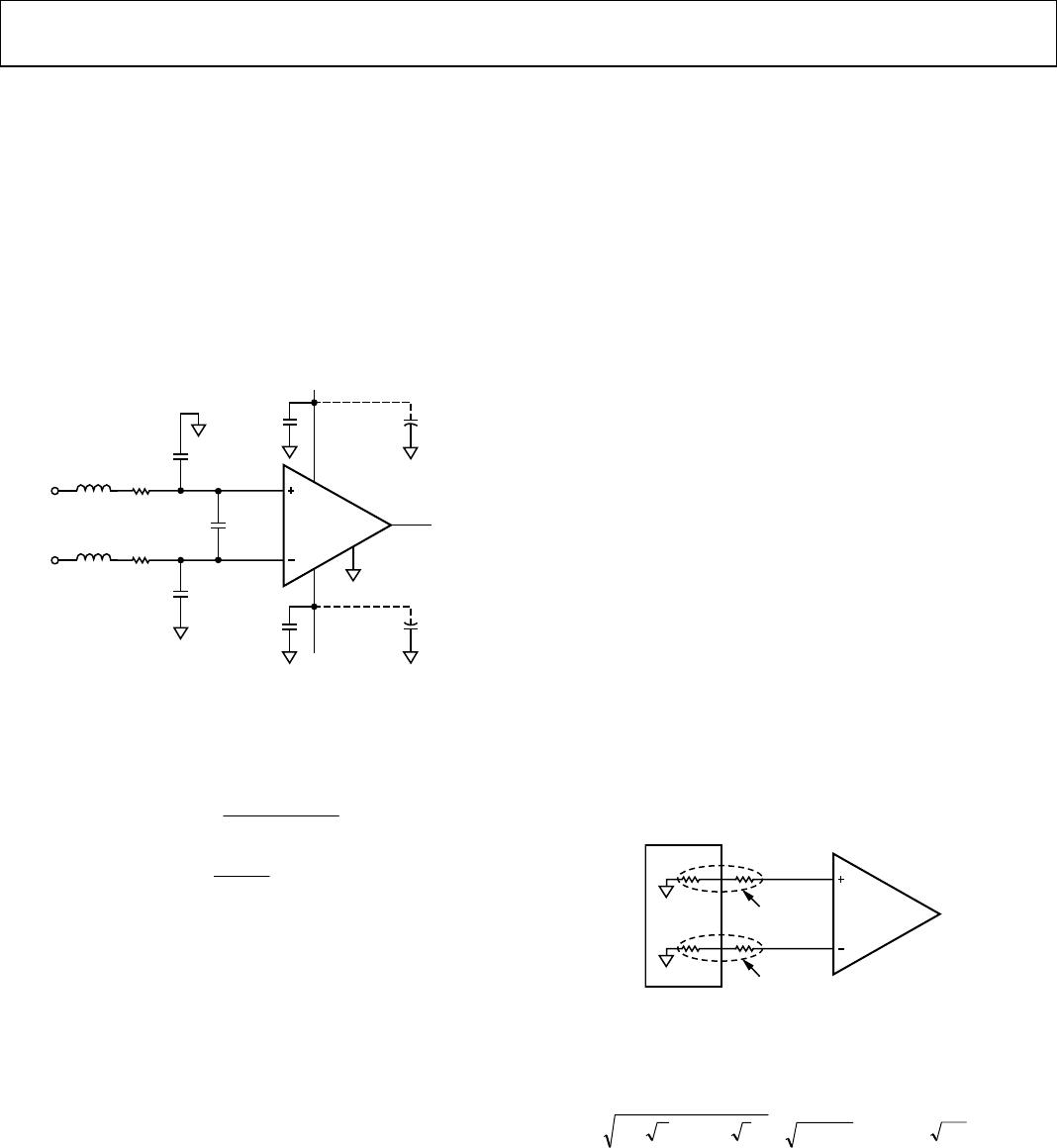
High frequency signals can be filtered with a low-pass filter
network at the input of the instrumentation amplifier, as shown
in Figure 44.
R
R
AD8428
+
V
S
+IN
–IN
0.1µF
10µF
10µF
0.1µF
REF
OUT
–V
S
C
D
10nF
C
C
1nF
C
C
1nF
33
33
09731-049
L*
L*
*CHIP FERRITE BEAD.
Figure 44. RFI Suppression
The filter limits both the differential and common-mode band-
width, as shown in the following equations:
)2(π2
1
C
D
DIFF
CCR
uencyFilterFreq
+
=
C
CM
RC
uencyFilterFreq
π2
1
=
where C
D
10 C
C
.
C
D
affects the differential signal, and C
C
affects the common-
mode signal. Choose values of R and C
C
that minimize RFI. A
mismatch between R × C
C
at the positive input and R × C
C
at
the negative input degrades the CMRR of the AD8428. By using
a value of C
D
one order of magnitude larger than C
C
, the effect
of the mismatch is reduced, and performance is improved.
Resistors add noise; therefore, the choice of resistor and capac-
itor values depends on the desired trade-off between noise, input
impedance at high frequencies, and RFI immunity. To achieve
low noise and sufficient RFI filtering, the use of inductive ferrite
beads is recommended (see Figure 44). Using inductive ferrite
beads allows the value of the resistors to be reduced, which helps
to minimize the noise at the input.
For best results, place the RFI filter network as close to the
amplifier as possible. Layout is critical to ensure that RF signals
are not picked up on the traces after the filter. If RF interference
is too strong to be filtered, shielding is recommended.
Note that the resistors used for the RFI filter can be the same
as those used for input protection (see the Input Protection
section).
CALCULATING THE NOISE OF THE INPUT STAGE
The total noise of the amplifier front end depends on much
more than the specifications in this data sheet. The three main
contributors to noise are as follows:
Source resistance
Voltage noise of the instrumentation amplifier
Current noise of the instrumentation amplifier
In the following calculations, noise is referred to the input (RTI);
that is, all sources of noise are calculated as if the source appeared
at the amplifier input. To calculate the noise referred to the ampli-
fier output (RTO), multiply the RTI noise by the gain of the
instrumentation amplifier.
Source Resistance Noise
Any sensor connected to the AD8428 has some output resistance.
There may also be resistance placed in series with the inputs for
protection from either overvoltage or radio frequency interference.
This combined resistance is labeled R1 and R2 in Figure 45. Any
resistor, no matter how well made, has an intrinsic level of noise.
This noise is proportional to the square root of the resistor value.
At room temperature, the value is approximately equal to
4 nV/√Hz × √(resistor value in k).
R2
R1
SENSO
R
AD8428
09731-050
Figure 45. Source Resistance from Sensor and Protection Resistors
For example, assuming that the combined sensor and protec-
tion resistance is 4 k on the positive input and 1 k on the
negative input, the total noise from the input resistance is
(
)
(
)
HznV/9.816641444
22
=+=×+×
Data Sheet AD8428
Rev. A | Page 17 of 20
Voltage Noise of the Instrumentation Amplifier Total Noise Density Calculation
Unlike other instrumentation amplifiers in which an external
resistor is used to set the gain, the voltage noise specification
of the AD8428 already includes the input noise, output noise,
and the R
G
resistor noise.
To determine the total noise of the in-amp, referred to input,
combine the source resistance noise, voltage noise, and current
noise contribution by the sum of squares method.
For example, if the R1 source resistance in Figure 45 is 4 k
and the R2 source resistance is 1 k, the total noise, referred
to input, is
Current Noise of the Instrumentation Amplifier
The contribution of current noise to the input stage in nV/√Hz
is calculated by multiplying the source resistance in k by the
specified current noise of the instrumentation amplifier in
pA/√Hz.
HznV/0.112.65.19.8
222
=++
For example, if the R1 source resistance in Figure 45 is 4 k
and the R2 source resistance is 1 k, the total effect from the
current noise is calculated as follows:
()()
HznV/2.625.2365.115.14
22
=+=×+×

AD8428ARZ

Mfr. #:
Manufacturer:
Description:
Instrumentation Amplifiers Low Noise Low Gain Drift
Lifecycle:
New from this manufacturer.
Delivery:
DHL FedEx Ups TNT EMS
Payment:
T/T Paypal Visa MoneyGram Western Union

Products related to this Datasheet