AD8428 Data Sheet
Rev. A | Page 18 of 20
APPLICATIONS INFORMATION
The classic 3-op-amp topology used for instrumentation
amplifiers typically places all the gain in the first stage and
subtracts the common-mode signals only in the second stage.
When operated at high gain, any amplifier is sensitive to large
interfering signals that can saturate it, thus making it impossible
to recover the signal of interest.
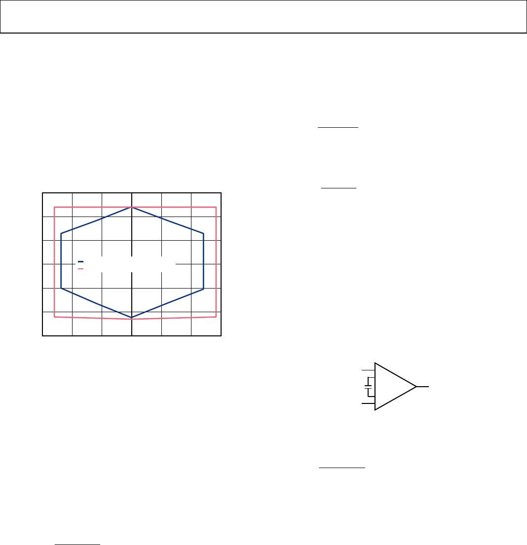
The AD8428 splits the total gain of 2000 into two stages: 200 in the
preamplification stage and 10 in the subtractor stage. Reducing the
gain of the first stage helps to increase the common-mode range
vs. differential signal range by avoiding saturation of the preamps.
–15
–10
–5
0
5
10
15
–15 –10 –5 0 5 10 15
INPUT COMMON-MODE VOLTAGE (V)
OUTPUT VOLTAGE (V)
SINGLE STAGE GAIN, G = 2000
AD8428
09731-246
Figure 46. AD8428 vs. Single Stage Gain Topology, G = 2000
In addition, filtering between stages can help to attenuate signals
before they reach the second amplification stage. This filtering
helps to prevent saturation of the second stage amplifier as long
as the signals are located in frequencies other than the signal of
interest.
EFFECT OF PASSIVE NETWORK ACROSS THE
FILTER TERMINALS
The AD8428 filter terminals allow access between the two
amplification stages. Adding a passive network between the two
terminals can shape the transfer function over the frequency of
the amplifier. The general expression for the transfer function is
represented by Equation 1.
6000
2000
+
×
=
Z(s)
Z(s)
G(s)
(1)
where Z(s) is the frequency dependent impedance of the
network across the filter terminals.
CIRCUITS USING THE FILTER TERMINALS
Setting the Amplifier to Different Gains
In its simplest form, the transfer function equation (Equation 1)
implies that the AD8428 can be configured for gains lower than
2000. This can be achieved by attaching a resistor across the filter
pins. Unlike the gain configuration of traditional instrumentation
amplifiers, this resistor attenuates the signal that was previously
amplified by the initial gain of 200.
Because this resistor appears inside the feedback of the subtractor
stage, it modifies the gain of the subtractor as well. The total gain
formula is a simplified version of the transfer function equation
(Equation 1).
6000
2000
+
×
=
G
G
R
R
G
(2)
The R
G
unit is in ohms. The resistor value required to obtain the
desired gain can be calculated using the following formula:
G
G
R
G
×
=
2000
6000
The AD8428 defaults to G = 2000 when no gain resistor is used.
When setting the amplifier to a different gain, the absolute gain
accuracy is only 10%. In addition, the temperature mismatch of
the external gain resistor increases the gain drift of the instrumen-
tation amplifier. Gain error and gain drift are at a guaranteed
minimum when a gain resistor is not used. For applications that
require accuracy at different gains, low noise, and wide bandwidth,
the AD8429 should be considered.
Low-Pass Filter
To help limit undesired differential signals, a first-order, low-pass
filter can be implemented by adding a capacitor across the filter
terminals of the AD8428, as shown in Figure 47.
+IN
–IN
+
AD8428
OUT
C
F
+FIL
–FIL
09731-146
Figure 47. Differential Low-Pass Filter
This single-pole filter limits the signal bandwidth, as shown in
the following equation:
F
C
C
f
)k6(2
1
Ωπ
=
The 6 k factor comes from the internal resistor values. The
tolerance of these resistors is 10%; therefore, using capacitors
with a tolerance better than 5% does not provide a significant
improvement on the absolute tolerance of the cutoff frequency.
Limiting the bandwidth of the amplifier also helps to minimize
the amount of out-of-band noise present at the output.
Note that filtering common-mode signals by adding a capacitor
on each filter terminal to ground degrades the performance of
the amplifier. This practice is generally discouraged because it
degrades CMRR performance. In addition, filtering common-
mode signals has little effect on preventing the saturation of the
internal nodes. On the contrary, the load added to the preamplifiers
causes them to saturate with even smaller common-mode signals.
Data Sheet AD8428
Rev. A | Page 19 of 20
Notch Filter
In cases where the frequency of the interfering signal is well
known, a notch filter can be implemented to help minimize the
impact of the known signal on the measurement. The filter can
be realized by adding a series LC network between the filter
pins, as shown in Figure 48.
+
AD8428
OUT
C
F
+FIL
–FIL
L
F
09731-147
Figure 48. Notch Filter Example
The inductor and capacitor form a resonant circuit that rejects
frequencies near the notch. The center frequency can be
calculated using the following equation:
FF
N
CL
f
π
=
2
1
The Q factor of the filter is given by the following equation:
F
F
C
L
Q
6000
1
=
The accuracy of the center frequency, f
N
, depends only on the
tolerance of the capacitor and inductor values, not on the value
of the internal resistors. However, the Q of the circuit depends on
both the tolerance of the external components and the absolute
tolerance of the internal resistors, which is typically 10%.
The Q factor is a filter parameter that indicates how narrow the
notch filter is. It is defined as follows:
A
B
N
ff
f
Q
=
where
f
A
and f
B
are the frequencies at which there is −3 dB
attenuation on each side of the notch.
This equation indicates that the higher the Q, the narrower the
notch—that is, high values of Q increase the selectivity of the
notch. In other words, although high values of Q reduce the
effect of the notch on the amplitude and phase in neighboring
frequencies, the ability to reject the undesired frequency may
also be reduced due to mismatch between it and the actual
center frequency. This mismatch can be caused by frequency
variations on the affecting source and the tolerance of the filter
inductor and capacitor values.
In contrast, low values of Q work better to ensure that the
interfering frequency is attenuated, but these low values also
affect the signal of interest if it is located close to the center
frequency of the notch.
For example, if the goal is to attenuate the interfering signal by
20 dB, a large Q value reduces the frequency range where the
notch is effective, as shown in Figure 49.
In contrast, a small Q value increases the range for the same
attenuation, which relaxes the tolerance requirements between
the inductor and capacitor and the frequency uncertainty of the
undesired signal. However, the lower Q value has a significant
effect on signal bandwidth one decade before the notch
frequency.
72
66
60
54
36
0.01f
N
0.1f
N
f
N
10f
N
100f
N
MAGNITUDE (dB)
FREQUENCY (Hz)
48
42
Q = 0.1
Q = 1
09731-249
–3dB
–20dB
Figure 49. Notch Filter Attenuation with Q = 0.1 and Q = 1
Around the Center Frequency
The maximum attenuation that can be achieved with a notch
filter is at its center frequency, f
N
. This maximum attenuation
(or depth of the notch) depends on the equivalent series
resistance of the inductor and capacitor at the center frequency.
Choosing components with high quality factors improves the
rejection at the filter’s center frequency. For information about
calculating the maximum allowed series resistance at the frequency
of interest to obtain the desired attenuation, see the Setting the
Amplifier to Different Gains section.
Extracting the Common-Mode Voltage of the Input
The common-mode signal present at the input terminals can be
extracted by inserting two resistors between the filter terminals
and tapping from the center, as shown in Figure 50. The common-
mode voltage, V
CM
, is the average of the voltages present at the
two inputs minus a 0.6 V drop.
+IN
–IN
+
AD8428
OUT
R
+FIL
–FIL
R
V
CM
09731-148
Figure 50. Extracting the Common-Mode Voltage
Use resistor values that are high enough to minimize the impact
on gain accuracy. For example, resistor values of 2 M introduce
an additional gain error of less than 0.2%. For information about
the impact of these resistors on the gain of the amplifier, see the
Effect of Passive Network Across the Filter Terminals section.
AD8428 Data Sheet
Rev. A | Page 20 of 20
OUTLINE DIMENSIONS
CONTROLLING DIMENSIONS ARE IN MILLIMETERS; INCH DIMENSIONS
(IN PARENTHESES) ARE ROUNDED-OFF MILLIMETER EQUIVALENTS FOR
REFERENCE ONLY AND ARE NOT APPROPRIATE FOR USE IN DESIGN.
COMPLIANT TO JEDEC STANDARDS MS-012-AA
012407-A
0.25 (0.0098)
0.17 (0.0067)
1.27 (0.0500)
0.40 (0.0157)
0.50 (0.0196)
0.25 (0.0099)
45°
1.75 (0.0688)
1.35 (0.0532)
SEATING
PLANE
0.25 (0.0098)
0.10 (0.0040)
4
1
85
5.00 (0.1968)
4.80 (0.1890)
4.00 (0.1574)
3.80 (0.1497)
1.27 (0.0500)
BSC
6.20 (0.2441)
5.80 (0.2284)
0.51 (0.0201)
0.31 (0.0122)
COPLANARITY
0.10
Figure 51. 8-Lead Standard Small Outline Package [SOIC_N]
Narrow Body
(R-8)
Dimensions shown in millimeters and (inches)
ORDERING GUIDE
Model
1
Temperature Range Package Description Package Option
AD8428ARZ −40°C to +85°C 8-Lead SOIC_N R-8
AD8428ARZ-RL −40°C to +85°C 8-Lead SOIC_N, 13” Tape and Reel R-8
AD8428BRZ −40°C to +85°C 8-Lead SOIC_N R-8
AD8428BRZ-RL −40°C to +85°C 8-Lead SOIC_N, 13” Tape and Reel R-8
1
Z = RoHS Compliant Part.
©2011–2012 Analog Devices, Inc. All rights reserved. Trademarks and
registered trademarks are the property of their respective owners.
D09731-0-4/12(A)

AD8428ARZ

Mfr. #:
Manufacturer:
Description:
Instrumentation Amplifiers Low Noise Low Gain Drift
Lifecycle:
New from this manufacturer.
Delivery:
DHL FedEx Ups TNT EMS
Payment:
T/T Paypal Visa MoneyGram Western Union

Products related to this Datasheet