Expand menu
Hello, Sign in
My Account
0
Cart
Home
Products
Sensors
Semiconductors
Passive Components
Connectors
Power
Electromechanical
Optoelectronics
Circuit Protection
Integrated Circuits - ICs
Main Products
Manufacturers
Blog
Services
About OMO
About Us
Contact Us
Check Stock
AD8428ARZ
P1-P3
P4-P6
P7-P9
P10-P12
P13-P15
P16-P18
P19-P21
AD8428
Data Sheet
Rev. A | Page 6 o
f 20
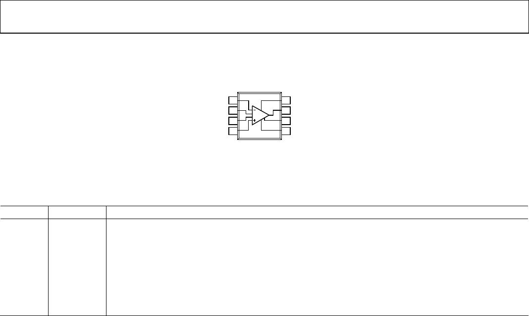
PIN CONFIGURA
TION AND FU
NCTION DESCRIPTIONS
–IN
1
–FI
L
2
+FIL
3
+IN
4
+V
S
8
OUT
7
REF
6
–V
S
5
A
D8428
TOP VI
EW
(No
t to
Scal
e)
09731-0
02
Figure 2. Pin Configuration
Table 5. Pin Funct
ion Descriptions
Pin No
.
Mnemonic
Description
1 −IN
Negative
Input
T
erminal.
2 −FIL
Negative
Filter
T
erminal.
3 +FIL
Positive
F
ilter
T
erminal.
4 +IN
Positiv
e
Input
T
erminal.
5 −V
S
Negativ
e Power Supply
T
erminal.
6
REF
R
eference
V
oltage T
erminal. Drive this terminal with
a low impedance voltage source to level-shift the output.
7 OUT
Output
T
erminal.
8 +V
S
Pos
it
i
v
e Po
we
r
S
u
pp
l
y
T
e
r
m
i
na
l
.
Data Sheet
AD8428
Rev. A | Page 7 o
f 20
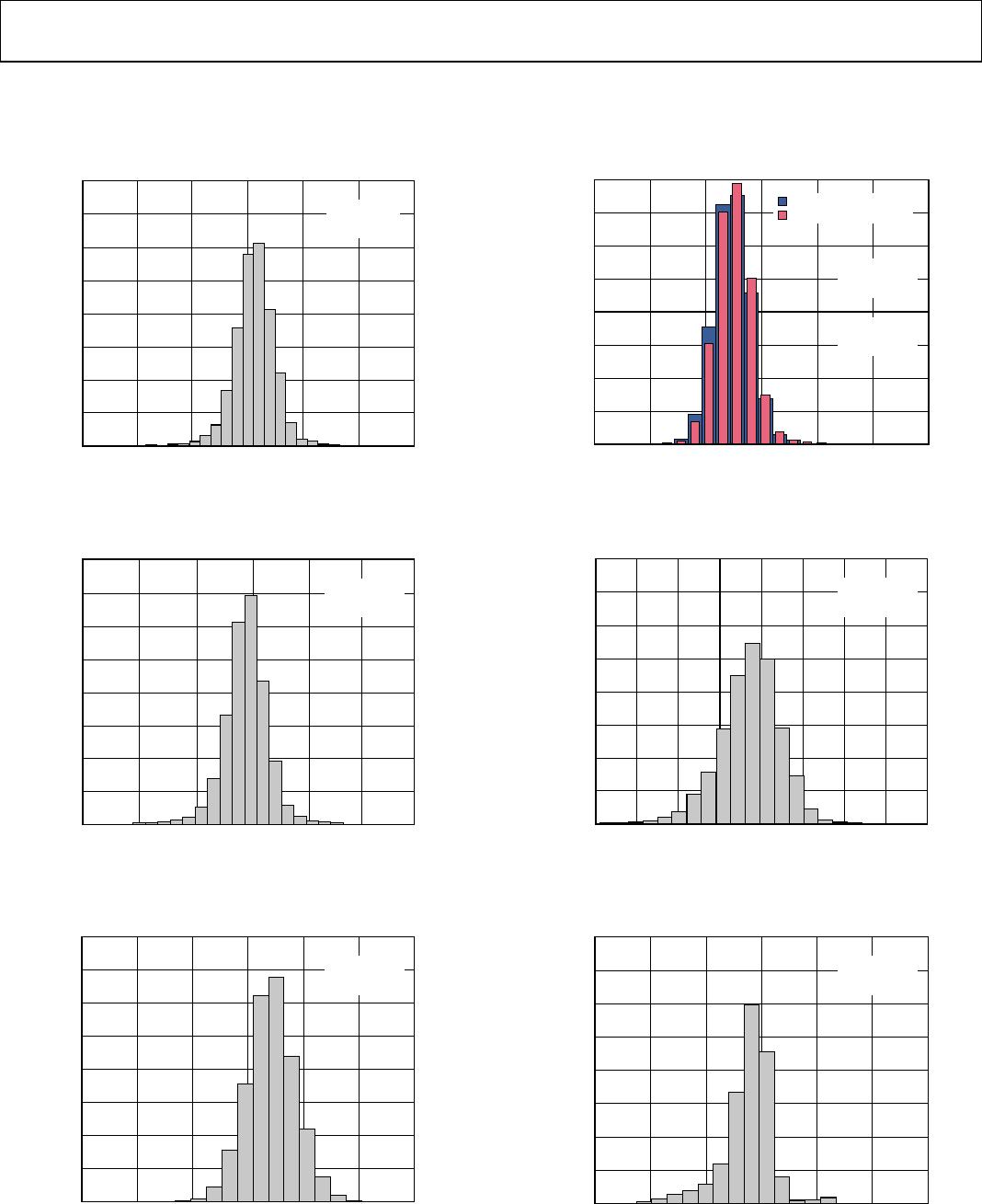
TYPICAL PERFORMANCE CHARACTE
RISTICS
V
S
= ±15 V
, V
REF
= 0 V
, T
A
= 25°C, G = 2000, R
L
= 10 k, unless o
ther
wise noted.
1200
1400
1600
1000
800
600
400
200
0
–40
–60
–20
40
60
20
0
HIT
S
V
OSI
(µV)
09731-00
3
N = 5170
MEAN = 2.
12
SD = 7.33
2
Figure 3. Typical D
istribution
of I
nput Offset
Voltage, V
S
= ±5 V
1400
1200
1000
800
600
400
200
0
–40
–60
–20
40
60
20
0
HIT
S
V
OSI
(µV)
09731-0
04
1600
N = 5169
MEAN =
–2.
57
SD = 7.
31066
Figure 4. Typical D
istribution
of I
nput Offset
Voltage, V
S
= ±15 V
1600
1400
1200
1000
800
600
400
200
0
–3
–2
–1
3
12
0
HIT
S
V
OSI
DRIF
T (
µV/
°C)
09731-0
05
N = 5166
MEAN =
0.3
98
SD = 0.
42707
Figure 5. Typical D
istribution
of I
nput Offset
Voltage Drift
1600
1400
1200
1000
800
600
400
200
0
–60
–40
–20
40
60
20
0
HIT
S
I
BI
AS
(nA)
09731-006
POSIT
IVE INPUT I
BI
AS
NEGA
TIVE
INPUT I
BI
AS
N = 5171
MEAN =
–10.
8
SD = 6.67496
N = 5171
MEAN =
–10.
2
SD = 6.52901
Figure 6. Typical D
istributi
on of Input
Bias Current
1000
1200
1400
1600
800
600
400
200
0
–8
–6
–4
6
8
04
2
–2
HIT
S
I
OS
(nA)
09731-0
07
N = 5171
MEAN =
–0.
53
SD = 1.
41655
Figure 7. Typical Di
stribution of Input Offset Current
1200
1400
1600
1000
800
600
400
200
0
–600
–400
200
400
600
0
–200
HIT
S
GAI
N ER
ROR (
µV
/V
)
09731-008
N = 3487
MEAN =
–53.
9
SD = 86
.
777
4
Figure 8. Typical D
istribution of Ga
in Error, Gain =
2000,
V
S
= ±15 V, R
L
= 10 kΩ
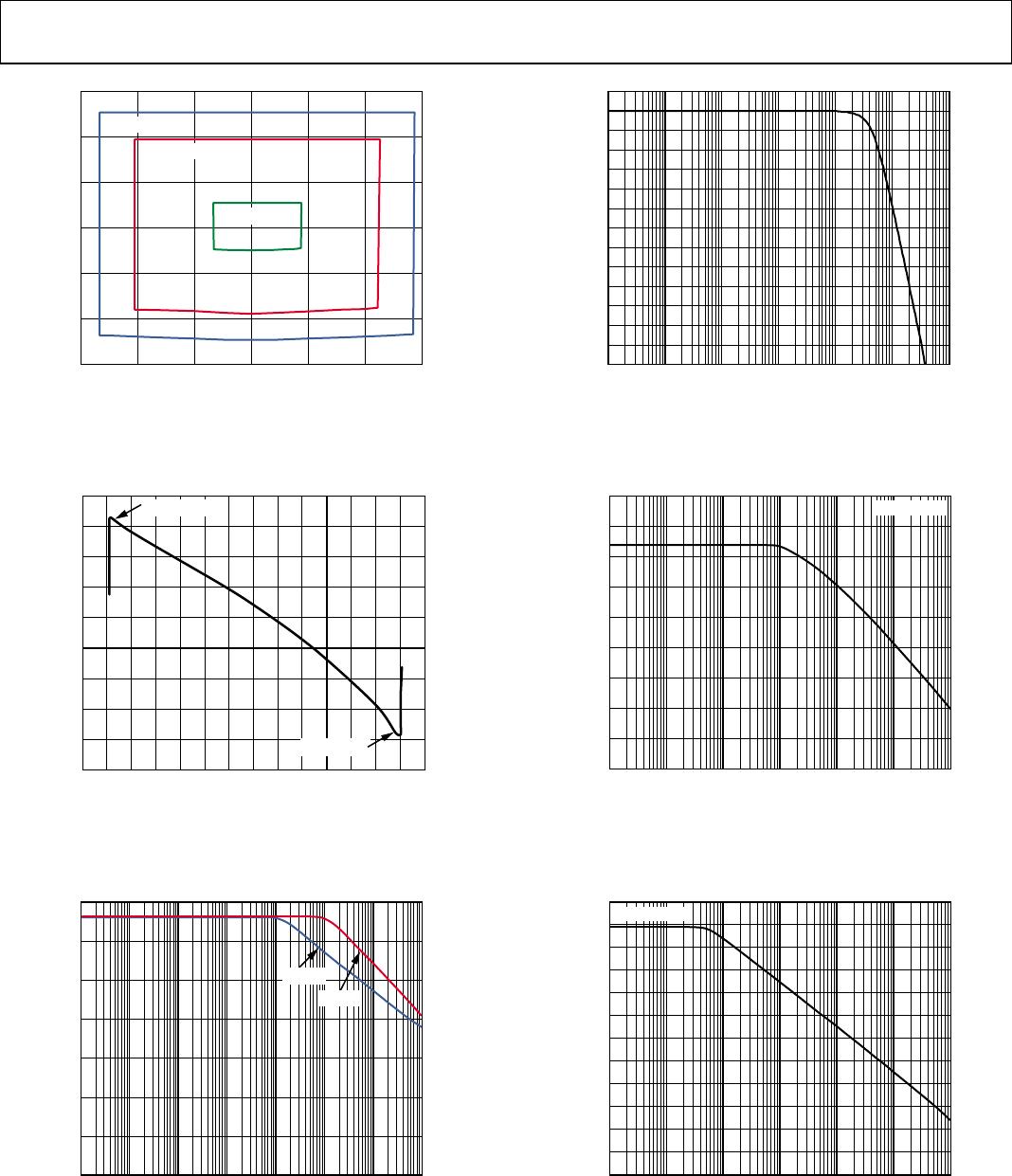
AD8428
Data Sheet
Rev. A | Page 8 o
f 20
15
10
5
0
–15
–10
–5
–15
–10
–5
0
5
10
15
INPU
T COMMON-
MODE VOLTA
GE (V)
OUTPU
T VOLTAGE (V)
09731-009
V
S
= ±15V
V
S
= ±12V
V
S
= ±5V
Figure 9. Input Comm
on-Mode Volta
ge vs. Output Voltage,
V
S
= ±5 V, V
S
= ±12 V, V
S
= ±15 V
18
0
–14
14
INPUT
BI
AS CURRENT
(n
A)
COMMON-MODE VOLTAGE (V)
09731-
010
2
4
6
8
10
12
14
16
–
1
2
–
1
0
–
8
–
6
–
4
–
2
02468
1
0
1
2
V
CM
= –11.8
V
V
CM
= +12V
Figure 10. Input Bi
as Current vs. Co
mmon-Mode Voltag
e,
V
S
= ±15 V
140
0
0.1
1
1M
100k
10k
1k
100
10
PSRR (d
B)
FREQ
UENCY (Hz
)
09731-0
11
20
40
60
80
100
120
+PSRR
–PSRR
Figure 11. PSRR vs. Frequency
72
–12
100
1k
10
k
100k
100M
1M
10M
GAIN
(dB)
FREQU
ENCY (H
z)
09731-0
14
–6
0
6
12
18
24
30
36
42
48
54
60
66
Figure 12. Gain vs. Frequency
170
80
1
10
100
1k
10k
100k
1M
CMRR (d
B)
FREQ
UENCY (Hz
)
09731-015
90
100
GAIN
= 200
0
110
120
130
140
150
160
Figure 13. CMRR vs. Frequency
120
0
1
10
100
1k
10k
100k
1M
CMRR (d
B)
FREQ
UENCY (Hz
)
09731-016
10
20
30
40
50
60
70
80
90
100
110
GAI
N = 2000
Figure 14. CMRR vs. Frequ
ency, 1 kΩ Source Imb
alance
P1-P3
P4-P6
P7-P9
P10-P12
P13-P15
P16-P18
P19-P21
AD8428ARZ
Mfr. #:
Buy AD8428ARZ
Manufacturer:
Description:
Instrumentation Amplifiers Low Noise Low Gain Drift
Lifecycle:
New from this manufacturer.
Delivery:
DHL
FedEx
Ups
TNT
EMS
Payment:
T/T
Paypal
Visa
MoneyGram
Western
Union
Products related to this Datasheet
AD8428ARZ-RL
AD8428BRZ-RL
AD8428ARZ
AD8428BRZ