LTC6240/LTC6241/LTC6242
19
624012fe
Amplifi er Characteristics
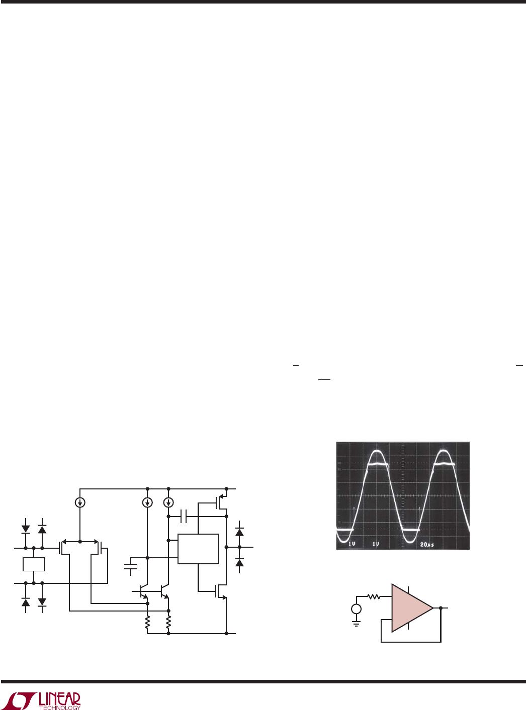
Figure 1 is a simplifi ed schematic of the amplifi er, which
has a pair of low noise input transistors M1 and M2. A
simple folded cascode Q1, Q2 and R1, R2 allow the input
stage to swing to the negative rail, while performing level
shift to the differential drive generator. Low offset voltage
is accomplished by laser trimming the input stage.
Capacitor C1 reduces the unity cross frequency and im-
proves the frequency stability without degrading the gain
bandwidth of the amplifi er. Capacitor CM sets the overall
amplifi er gain bandwidth. The differential drive generator
supplies signals to transistors M3 and M4 that swing the
output from rail-to-rail.
The photo of Figure 2 shows the output response to an
input overdrive with the amplifi er connected as a voltage
follower. If the negative going input signal is less than
a diode drop below V
, no phase inversion occurs. For
input signals greater than a diode drop below V
, limit the
current to 3mA with a series resistor R
S
to avoid phase
inversion.
ESD
The LTC6240/LTC6241/LTC6242 have reverse-biased ESD
protection diodes on all input and outputs as shown in
Figure 1. If these pins are forced beyond either supply,
unlimited current will fl ow through these diodes. If the
current is transient and limited to one hundred milliamps
or less, no damage to the device will occur.
The amplifi er input bias current is the leakage current of
these ESD diodes. This leakage is a function of the tempera-
ture and common mode voltage of the amplifi er, as shown
in the Typical Performance Characteristics curves.
Noise
The LTC6240/LTC6241/LTC6242 exhibit exceptionally
low 1/f noise in the 0.1Hz to 10Hz region. This 550nV
P-P
noise allows these op amps to be used in a wide variety
of high impedance low frequency applications, where
zero-drift amplifi ers might be inappropriate due to their
charge injection.
In the frequency region above 1kHz the LTC6240/LTC6241/
LTC6242 also show good noise voltage performance. In
this frequency region, noise can easily be dominated by
the total source resistance of the particular application.
Specifi cally, these amplifi ers exhibit the noise of a 3.1k
resistor, meaning it is desirable to keep the source and
feedback resistance at or below this value, i.e. R
S
+ R
G
||R
FB
≤ 3.1k. Above this total source impedance, the noise
voltage is not dominated by the amplifi er.
Noise current can be estimated from the expression i
n
=
2qI
B
, where q = 1.6 • 10
–19
coulombs. Equating √4kTRΔf
and R√2qI
B
Δf shows that for source resistors below 50G
the amplifi er noise is dominated by the source resistance.
See the Typical Performance Characteristics curve Noise
Current vs Frequency.
Figure 1. Simplifi ed Schematic Figure 2. Unity Gain Follower Test Circuit
APPLICATIONS INFORMATION
R2
Q2
6241 F01
V
IN
+
I
TAIL
V
IN
V
O
V
+
V
+
V
V
V
CM
DESD5
DIFFERENTIAL
DRIVE
GENERATOR
BIAS
DESD6
V
+
DESD2
V
+
DESD4
V
DESD1
V
DESD3
R1
Q1
M2M1
M3
M4
C1
CLAMP
+2.5V
–2.5V
6241 F02
+
LTC6240
R
S
V
IN
V
OUT
V
OUT
AND V
IN
OF FOLLOWER WITH LARGE INPUT OVERDRIVE
V
DD
=
+2.5V
V
SS
=
–2.5V
LTC6240/LTC6241/LTC6242
20
624012fe
Proprietary design techniques are used to obtain simulta-
neous low 1/f noise and low input capacitance. Low input
capacitance is important when the amplifi er is used with
high value source and feedback resistors. High frequency
noise from the amplifi er tail current source, I
TAIL
in Fig-
ure 1, couples through the input capacitance and appears
across these large source and feedback resistors. As an
example, the photodiode amplifi er of Figure 15 on the last
page of this data sheet shows the noise results from the
LTC6241 and the results of a competitive CMOS amplifi er.
The LTC6241 output is the ideal noise of a 1M resistor
at room temperature, 130nV√Hz.
Half the Noise
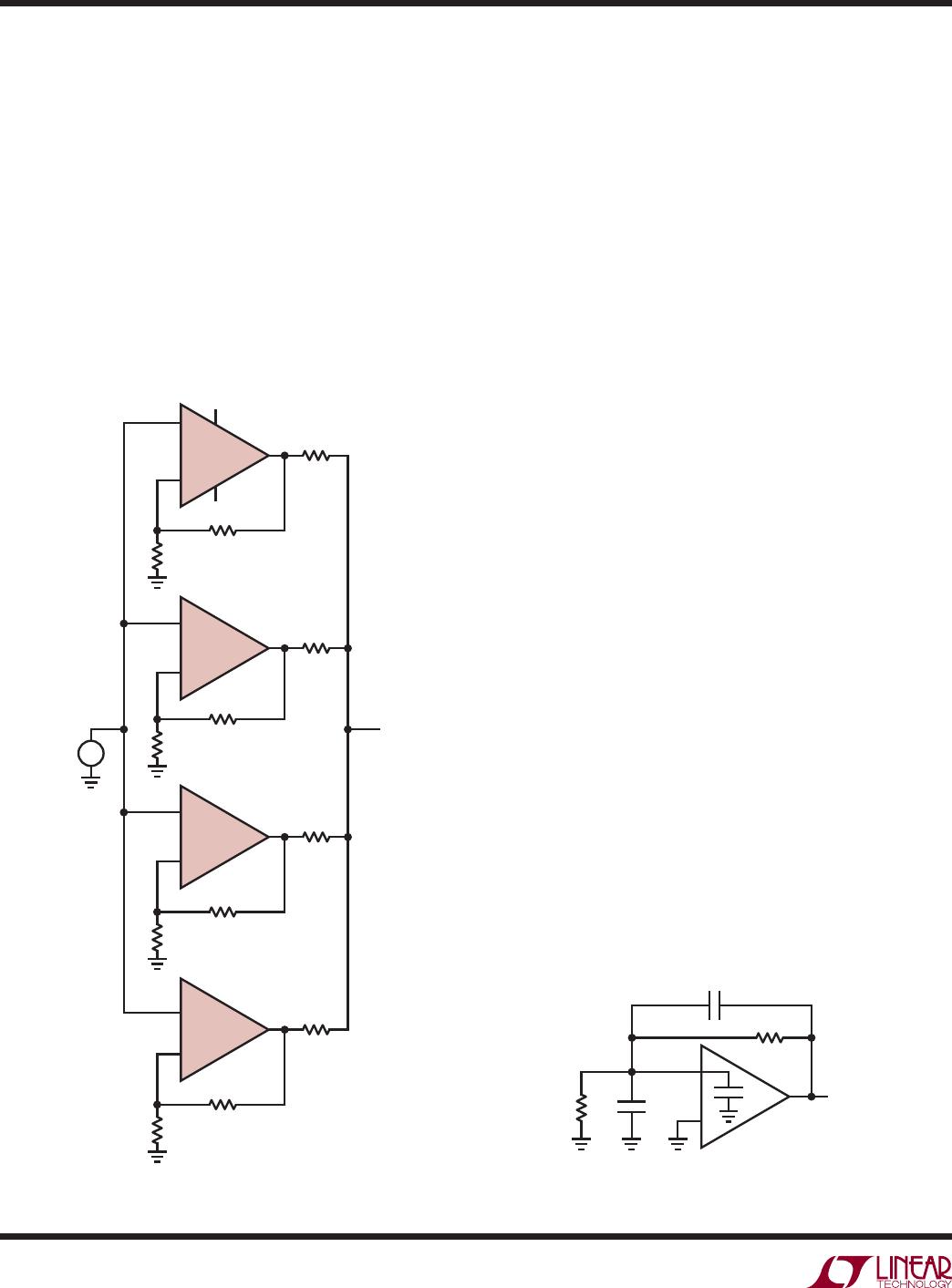
The circuit shown in Figure 3 can be used to achieve even
lower noise voltage. By paralleling 4 amplifi ers the noise
voltage can be lowered by √4, or half as much noise. The
comes about from an RMS summing of uncorrelated
noise sources. This circuit maintains extremely high input
resistance, and has a 250 output resistance. For lower
output resistance, a buffer amplifi er can be added without
infl uencing the noise.
Stability
The good noise performance of these op amps can be at-
tributed to large input devices in the differential pair. Above
several hundred kilohertz, the input capacitance rises and
can cause amplifi er stability problems if left unchecked.
When the feedback around the op amp is resistive (R
F
), a
pole will be created with R
F
, the source resistance, source
capacitance (R
S
, C
S
), and the amplifi er input capacitance.
In low gain confi gurations and with R
F
and R
S
in even
the kilohm range (Figure 4), this pole can create excess
phase shift and possibly oscillation. A small capacitor C
F
in parallel with R
F
eliminates this problem.
Low Noise Single-Ended Input to Differential Output
Amplifi er
The circuit on the fi rst page of the data sheet is a low noise
single-ended input to differential output amplifi er, with a
200k input impedance. The very low input bias current
of the LTC6241 allows for these large input and feedback
resistors. The 200k resistors, R1 and R2, along with C1 and
C2 set the –3dB bandwidth to 80kHz. Capacitor C3 is used
to cancel effects of input capacitance, while C4 adds phase
lead to compensate the phase lag of the second amplifi er.
Figure 3. Parallel Amplifi er Lowers Noise by 2x Figure 4. Compensating Input Capacitance
APPLICATIONS INFORMATION
10Ω
6241 F03
+
1/4
LTC6242
1k
1k
10Ω
+
1/4
LTC6242
1k
1k
10Ω
+
1/4
LTC6242
1k
1k
10Ω
+
1/4
LTC6242
1k
1k
+2.5
–2.5
V
IN
V
O
+
C
IN
C
S
6241 F04
R
F
R
S
OUTPUT
C
F
LTC6240/LTC6241/LTC6242
21
624012fe
The op amp’s good input offset voltage match and low
input bias current means that the typical differential output
offset voltage is less than 40µV. A noise spectrum plot of
the differential output is shown in Figure 5.
The guard ring should extend as far as necessary to shield
the high impedance signal from any and all leakage paths.
Figure 6 shows the use of a guard ring on the LTC6241 in
a unity gain confi guration. In this case the guard ring is
connected to the output and is shielding the high impedance
noninverting input from V
. Figure 7 shows the inverting
gain confi guration.
A Digitally Programmable AC Difference Amplifi er
The LTC6241 confi gured as a difference amplifi er, can be
combined with a programmable gain amplifi er (PGA) to
obtain a low noise high speed programmable difference
amplifi er. Figure 8 shows the LTC6241 based as a single-
supply AC amplifi er. One LTC6241 op amp is used at the
circuit’s input as a standard four resistor difference amplifi er.
Figure 5. Differential Output Noise
Achieving Low Input Bias Current
The DD package is leadless and makes contact to the PCB
beneath the package. Solder fl ux used during the attach-
ment of the part to the PCB can create leakage current
paths and can degrade the input bias current performance
of the part. All inputs are susceptible because the backside
paddle is connected to V
internally. As the input voltage
changes or if V
changes, a leakage path can be formed
and alter the observed input bias current. For lowest bias
current, use the LTC6240/LTC6241 in the SO-8 and provide
a guard ring around the inputs that are tied to a potential
near the input voltage.
Layout Considerations and a PCB Guard Ring
In high source impedance applications such as pH probes,
photodiodes, strain gauges, et cetera, the low input bias
current of these parts requires a clean board layout to
minimize additional leakage current into a high impedance
signal node. A mere 100G of PC board resistance
between a 5V supply trace and an input trace adds 50pA
of leakage current, far greater then the input bias current
of the operational amplifi er. A guard ring around the high
impedance input traces driven by a low impedance source
equal to the input voltage prevents such leakage problems.
Figure 6. Sample Layout. Unity Gain Confi guration, Using Guard
Ring to Shield High Impedance Input from Board Leakage
Figure 7. Sample Layout. Inverting Gain Confi guration, Using
Guard Ring to Shield High Impedance Input from Board Leakage
APPLICATIONS INFORMATION
FREQUENCY (kHz)
020 6010 40 8030 7050 90 100
DIFFERENTIAL OUTPUT VOLTAGE DENSITY (nV/√Hz)
140
60
80
100
120
0
20
40
6241 F05
V
S
= ±2.5V
T
A
= 25°C
–3dB BW = 80kHz
LTC6241 S8
R
OUT
+
IN
IN
+
V
LEAKAGE
CURRENT
NO LEAKAGE
CURRENT
GUARD
RING
NO SOLDER MASK
OVER THE GUARD RING
LTC6241 F06
LTC6241 S8
LTC6241 F07
R
R
OUT
+
IN
IN
+
V
V
IN
GND

LTC6240CS5#TRMPBF

Mfr. #:
Manufacturer:
Analog Devices Inc.
Description:
Precision Amplifiers 1x 18MHz, L N, R2R Out, CMOS Op Amp
Lifecycle:
New from this manufacturer.
Delivery:
DHL FedEx Ups TNT EMS
Payment:
T/T Paypal Visa MoneyGram Western Union