LTC6240/LTC6241/LTC6242
25
624012fe
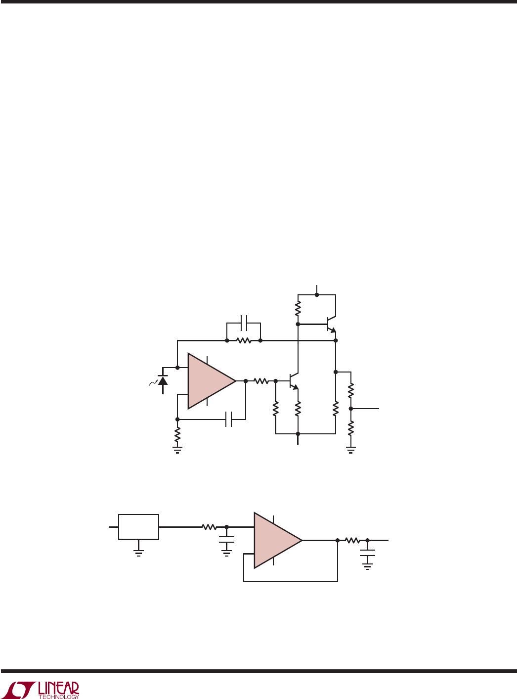
1M Transimpedance Amplifi er with 43nV/√Hz
Output Noise
In a normal 1M transimpedance amplifi er, like that shown
on the back page of this data sheet, the output noise density
must be at least 130nV/√Hz at room temperature. This is
true even should the op amp be perfectly noiseless, because
the 1M resistor provides 130nV/√Hz of voltage noise at
room temperature independently of the op amp.
The circuit of Figure 13 provides an overall transimpedance
gain of 1M, but it has an output noise density of only
43nV/√Hz, about 1/3 of the normal transimpedance ampli-
fi er. It does this by taking a higher initial transimpedance
gain of 10M and then attenuating by a factor of 10. The
transistor section provides voltage gain and works on a
54V supply voltage to guarantee adequate output swing.
By achieving an output swing of 50V before attenuation,
the circuit provides an output swing to 5V after attenu-
ation. The 10M resistor sets the gain of the TIA stage
and has a noise density of 400nV/√Hz. After attenuation,
the effective TIA gain drops to 1M while the noise fl oor
drops to 40nV/√Hz, which clearly dominates the observed
43nV/√Hz. Note the additional benefi t that the offset voltage
of the op amp is divided by 10. Worst-case output offset
for this circuit is 150µV over temperature.
Reference Buffer
Figure 14 shows the LTC6240 being utilized as a buffer
in conjunction with the LT1019 reference. The passive
R-C fi lter attenuates the reference noise and the LTC6240
provides a low noise buffer, resulting in an output noise
of 8nV/√Hz.
Figure 13. 1M Transimpedance Amplifi er with 43nV/√Hz Output Noise
Figure 14. Low Noise Reference Buffer
APPLICATIONS INFORMATION
5V
54V
–5V
–1.5V
3pF
PHOTODIODE
6241 F13
–5V
10k
–
+
LTC6240HV
100pF
10M
1%
0.3pF
1k
10k 2.4k
33k
MPSA06
43k
9.09k
1%
1/4W
1k
1%
V
OUT
1M GAIN
(1V/µA)
10M GAIN
(10V/µA)
MPSA06
5V
–5V
6241 F14
0.2Ω
–
+
LTC6240HV
1M
10µF
CERAMIC
OR FILM
8nV/√Hz
V
OUT
1µF
LT1019-2.5
180nV/√Hz