LTC6240/LTC6241/LTC6242
22
624012fe
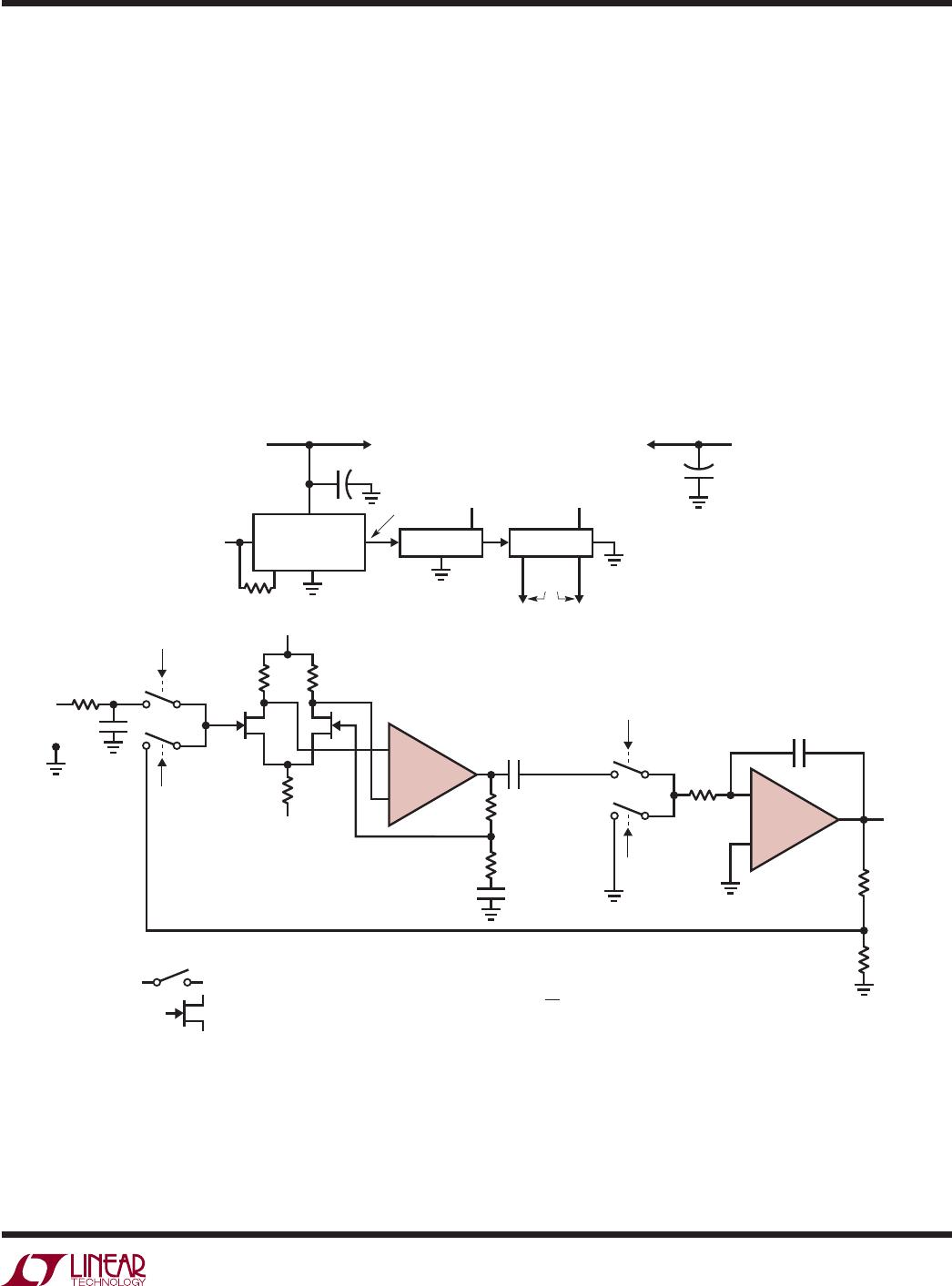
Figure 8. Wideband Difference Amplifi er with High
Input Impedance and Digitally Programmable Gain
The low bias current and current noise of the LTC6241
allow the use of high valued input resistors, 100k or
greater. Resistors R1, R2, R3 and R4 are equal and the
gain of the difference amplifi er is one. An LTC6910-2 PGA
amplifi es the difference amplifi er output with inverting
gains of –1, –2, –4, –8, –16, –32 and –64. The second
LTC6241 op amp is used as an integrator to set the DC
output voltage equal to the LT6650 reference voltage V
REF
.
The integrator drives the PGA analog ground to provide
a feedback loop, in addition to blocking any DC voltage
through the PGA. The reference voltage of the LT6650
can be set to a voltage from 400mV to V
+
– 350mV with
resistors R5 and R6. If R6 is 20k or less, the error due
to the LT6650 op amp bias current is negligible. The low
voltage offset and drift of the LTC6241 integrator will not
contribute any signifi cant error to the LT6650 reference
voltage. The LT6650 V
REF
voltage has a maximum error
of ±2% with 1% resistors. The upper –3dB frequency of
the amplifi er is set by resistor R3 and capacitor C1 and
is limited by the bandwidth of the PGA when operated at
a gain of 64. Capacitor C2 is equal to C1 and is added to
maintain good common mode rejection at high frequency.
The lower –3dB frequency is set by the integrator resistor
R7, capacitor C3, and the gain setting of the LTC6910-2
PGA. This lower –3dB zero frequency is multiplied by the
PGA gain. The rail-to-rail output of the LTC6910-2 PGA
allows for a maximum output peak-to-peak voltage equal
to twice the V
REF
voltage. At the maximum gain setting of
64, the maximum peak-to-peak difference between inputs
V1 and V2 is equal to twice V
REF
divided by 64.
Example Design: Design a programmable gain AC differ-
ence amplifi er, with a bandwidth of at least 10Hz to 100kHz,
an input impedance equal to or greater than 100k, and
an output DC reference equal to 1V.
a. Select input resistors R1, R2, R3 and R4 equal to
100k.
b. If the upper –3dB frequency is 100kHz then C1 = 1/(2π
• R2 • f3dB) = 1/(6.28 • 100k • 100kHz) = 15pF (to
the nearest 5% value) and C2 = C1 = 15pF.
c. Select R7 equal to one 1M and set the lower –3dB
frequency to 10Hz at the highest PGA gain of 64, then
C3 = Gain/(2π • R7 • f3dB) = 64/(6.28 • 100k • 10Hz)
= 1µF. Lower gains settings will give a lower f3dB.
d. Calculate the value of R5 to set the LT6650 reference
equal to 1V;
V
REF
= 0.4(R5/R6 + 1), so R5 = R6(2.5V
REF
– 1). For
R6 = 20k, R5 = 30k
With V
REF
= 1V the maximum input difference voltage
is equal to 2V/64 = 31.2mV.
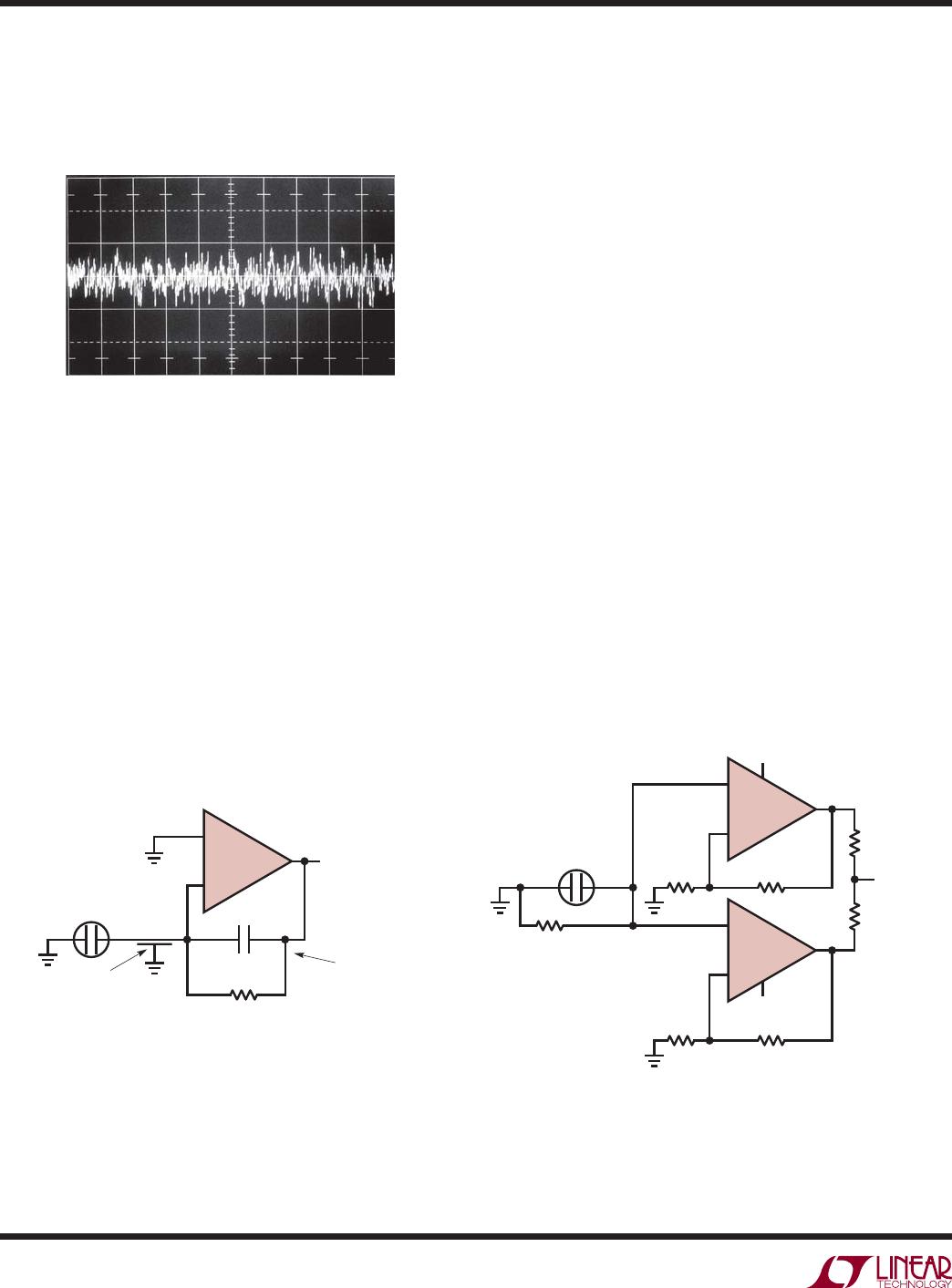
40nVpp Noise, 0.05μV/°C Drift, Chopped FET
Amplifi er
Figure 9’s circuit combines the ±5V rail-to-rail performance
of the LTC6241HV with a pair of extremely low noise JFETs
confi gured in a chopper based carrier modulation scheme
APPLICATIONS INFORMATION
6241 F08
R4
R3
R2
+
1/2
LTC6241
C1
C2
1µF
0.1µF
8 765
G2 G1 G0
1
1
2
234
AGNDOUT IN V
V
+
0.1µF
V
+
V
+
R1
R1 = R2 = R3 = R4
V2
V1
R5
1k
1000pF
3 4
5
R6
20k
LTC6910-2
LT6650
V
OUT
V
REF
+
1/2
LTC6241
C3
R7
100Ω
1µF
DIGITAL INPUTS
G1G2 GO
GAIN
0
0
1
1
0
0
1
1
0
0
0
0
1
1
1
1
0
1
0
1
0
1
0
1
0
–1
–2
–4
–8
–16
–32
–64
V
OUT
= (V1 – V2) GAIN + V
REF

V
R
R
RkV
REF
REF
=+
¥
§
¦
´
µ
=

=
04
5
6
1
510 5 2 R620
.•
•• k
d BANDWIDTH f f
f
RC
HIGH LOW
HIGH
––
••
3
1
23
=
=
P 1273
f
GAIN
RC
LOW
=
•• P
LTC6240/LTC6241/LTC6242
23
624012fe
Figure 9. Ultralow Noise Chopper Amplifi er
to achieve an extraordinarily low noise and low DC drift.
The performance of this circuit is suited for the demand-
ing transducer signal conditioning situations such as high
resolution scales and magnetic search coils.
The LTC1799’s output is divided down to form a 2-phase
925Hz square wave clock. This frequency, harmonically
unrelated to 60Hz, provides excellent immunity to harmonic
beating or mixing effects which could cause instabilities.
S1 and S2 receive complementary drive, causing A1 to
see a chopped version of the input voltage. A1’s square
wave output is synchronously demodulated by S3 and
S4. Because these switches are synchronously driven
with the input chopper, proper amplitude and polarity
information is presented to A2, the DC output amplifi er.
This stage integrates the square wave into a DC voltage,
providing the output. The output is divided down (R2 and
R1) and fed back to the input chopper where it serves as
a zero signal reference. Gain, in this case 1000, is set by
the R1-R2 ratio. Because A1 is AC coupled, its DC offset
and drift do not affect the overall circuit offset, resulting
in the extremely low offset and drift noted. The JFETs
have an input RC damper that minimizes offset voltage
contribution due to parasitic switch behavior, resulting in
the 1µV offset specifi cation.
APPLICATIONS INFORMATION
+
+
BIAS
10M
F
14
15
16
3
2
1
S4
S3
240k
F
OUTPUT
A2
LTC6241HV
A1
LTC6241HV
F
INPUT
10k
8
7
11
S1
S2
9
6
10
R2
10k
R1
10Ω
NOISE
OFFSET
DRIFT
OPEN-LOOP GAIN
I
= 40nV
P-P
0.1Hz TO 10Hz
= 1µV
= 0.05µV/°C
R2
10
= 10
= 500pA
+1
GAIN
=
9
0.01µF
Ø1
Ø1
Ø2
Ø2
6241 F09
= 0.1% METAL FILM RESISTOR
= 1% METAL FILM RESISTOR
*
**
= LTC201 QUAD
= LSK389
= LINEAR INTEGRATED SYSTEMS
FREMONT, CA
F
DIV
R
SET
LTC1799
V
+
74C90 ÷ 10
18.5kHz
OUT
74C74 ÷ 2
TO
Ø1
POINTS
TO
Ø2
POINTS
Q Q
54.2k*
TO LTC201 V
+
PIN
5V
5V
–5V
5V 5V
925Hz
TO LTC201 V
PIN
F
898Ω**
5V
–5V
898Ω**
LSK389
30.1Ω
499Ω**
+
+
LTC6240/LTC6241/LTC6242
24
624012fe
by the sensor is forced across the feedback capacitor
by the op amp action. Because the feedback capacitor
is 100 times smaller than the sensor, it will be forced to
100 times what would have been the sensors open circuit
voltage. So the circuit gain is 100. The benefi t of this ap-
proach is that the signal gain of the circuit is independent
of any cable capacitance introduced between the sensor
and the amplifi er. Hence this circuit is favored for remote
accelerometers where the cable length may vary. Diffi culties
with the circuit are inaccuracy of the gain setting with the
small capacitor, and low frequency cutoff due to the bias
resistor working into the small feedback capacitor.
Figure 12 shows a noninverting amplifi er approach. This
approach has many advantages. First of all, the gain is set
accurately with resistors rather than with a small capaci-
tor. Second, the low frequency cutoff is dictated by the
bias resistor working into the large 770pF sensor, rather
than into a small feedback capacitor, for lower frequency
response. Third, the noninverting topology can be paral-
leled and summed (as shown) for scalable reductions in
voltage noise. The only drawback to this circuit is that the
parasitic capacitance at the input reduces the gain slightly.
This circuit is favored in cases where parasitic input
capacitances such as traces and cables will be relatively
small and invariant.
The noise measured over a 50 second interval, in Figure 10,
is 40nV in a 0.1Hz to 10Hz bandwidth.This low noise is at-
tributed to the input JFETs die size and current density.
Figure 11. Classical Inverting Charge Amplifi er Figure 12. Low Noise Noninverting Shock Sensor Amplifi er
Figure 10. Noise in a 0.1Hz to 10Hz Bandwidth
Low Noise Shock Sensor Amplifi ers
Figures 11 and 12 show the amplifi ers realizing two dif-
ferent approaches to amplifying signals from a capacitive
sensor. The sensor in both cases is a 770pF piezoelectric
shock sensor accelerometer, which generates charge under
physical acceleration.
Figure 11 shows the classical “charge amplifi er” approach.
The LTC6240 is in the inverting confi guration so the sensor
looks into a virtual ground. All of the charge generated
APPLICATIONS INFORMATION
5s/DIV
6241 F10
20nV/DIV
BIAS RESISTOR
VISHAY-TECHNO
CRHV2512AF1007G
(OR EQUIVALENT)
MAIN
GAIN-SETTING
ELEMENT IS A
CAPACITOR
SHOCK SENSOR
MURATA-ERIE
PKGS-00LD
770pF
CABLE HAS
UNKNOWN C
R
f
1G
6241 F11
V
OUT
= 110mV/g
+
LTC6240
C
f
7.7pF
BIAS RESISTOR
VISHAY-TECHNO
CRHV2512AF1007G
(OR EQUIVALENT)
1G
V
S
+
6241 F12
10k
1k
1k
100Ω
V
OUT
= 110mV/g
V
S
= ±1.4V to ±5.5V
BW = 0.2Hz to 10kHz
V
OUT
+
1/2
LTC6241HV
V
S
10k100Ω
+
1/2
LTC6241HV
SHOCK SENSOR
MURATA-ERIE
PKGS-00LD
770pF

LTC6240CS5#TRMPBF

Mfr. #:
Manufacturer:
Analog Devices Inc.
Description:
Precision Amplifiers 1x 18MHz, L N, R2R Out, CMOS Op Amp
Lifecycle:
New from this manufacturer.
Delivery:
DHL FedEx Ups TNT EMS
Payment:
T/T Paypal Visa MoneyGram Western Union