1
®
FN6462.0
PX3511A, PX3511B
Advanced Synchronous Rectified Buck
MOSFET Drivers with Protection Features
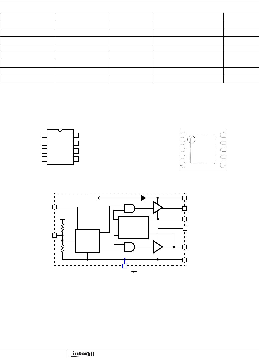
The PX3511A and PX3511B are high frequency MOSFET
drivers specifically designed to drive upper and lower power
N-Channel MOSFETs in a synchronous rectified buck
converter topology. These drivers combined with the
ISL6595 Digital Multi-Phase Buck PWM controller and
N-Channel MOSFETs form a complete core-voltage
regulator solution for advanced microprocessors.
The PX3511A drives the upper gate to 12V, while the lower
gate can be independently driven over a range from 5V to
12V. The PX3511B drives both upper and lower gates over a
range of 5V to 12V. This drive-voltage provides the flexibility
necessary to optimize applications involving trade-offs
between gate charge and conduction losses.
An adaptive zero shoot-through protection is integrated to
prevent both the upper and lower MOSFETs from conducting
simultaneously and to minimize the dead time. These
products add an overvoltage protection feature operational
before VCC exceeds its turn-on threshold, at which the
PHASE node is connected to the gate of the low side
MOSFET (LGATE). The output voltage of the converter is
then limited by the threshold of the low side MOSFET, which
provides some protection to the microprocessor if the upper
MOSFET(s) is shorted during initial start-up.
These drivers also feature a three-state PWM input which,
working together with Intersil’s multi-phase PWM controllers,
prevents a negative transient on the output voltage when the
output is shut down. This feature eliminates the Schottky
diode that is used in some systems for protecting the load
from reversed output voltage events.
Features
• Dual MOSFET Drives for Synchronous Rectified Bridge
• Adjustable Gate Voltage (5V to 12V) for Optimal Efficiency
• 36V Internal Bootstrap Schottky Diode
• Bootstrap Capacitor Overcharging Prevention
• Supports High Switching Frequency (up to 2MHz)
- 3A Sinking Current Capability
- Fast Rise/Fall Times and Low Propagation Delays
• Three-State PWM Input for Output Stage Shutdown
• Three-State PWM Input Hysteresis for Applications With
Power Sequencing Requirement
• Pre-POR Overvoltage Protection
• VCC Undervoltage Protection
• Expandable Bottom Copper Pad for Enhanced Heat
Sinking
• Dual Flat No-Lead (DFN) Package
- Near Chip-Scale Package Footprint; Improves PCB
Efficiency and Thinner in Profile
• Pb-Free Plus Anneal Available (RoHS Compliant)
Applications
• Core Regulators for Intel® and AMD® Microprocessors
• High Current DC/DC Converters
• High Frequency and High Efficiency VRM and VRD
Related Literature
• Technical Brief TB363 “Guidelines for Handling and
Processing Moisture Sensitive Surface Mount Devices
(SMDs)”
• Technical Brief TB417 for Power Train Design, Layout
Guidelines, and Feedback Compensation Design
Data Sheet February 26, 2007
CAUTION: These devices are sensitive to electrostatic discharge; follow proper IC Handling Procedures.
1-888-INTERSIL or 1-888-468-3774
| Intersil (and design) is a registered trademark of Intersil Americas Inc.
Copyright Intersil Americas Inc. 2006. All Rights Reserved
All other trademarks mentioned are the property of their respective owners.