Technical Note
BU7251G,BU7251SG, BU7231G,BU7231SG,
BU7252F/FVM,BU7252S F/FVM,BU7232F/FVM,BU7232S F/FVM
2/18
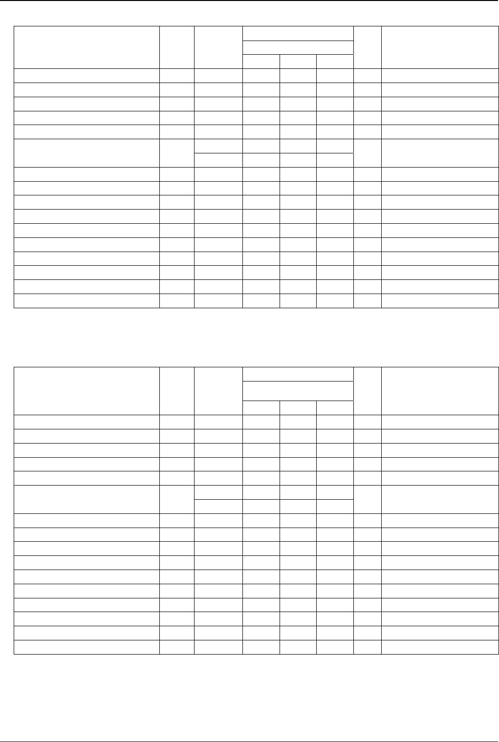
●Absolute maximum ratings (Ta=25[℃])
Parameter Symbol
Rating
Unit
BU7251G,BU7252 F/FVM
BU7231G,BU7232 F/FVM
BU7251SG,BU7252S F/FVM
BU7231SG,BU7232S F/FVM
Supply Voltage VDD-VSS +7 V
Differential Input Voltage
(*1)
Vid VDD-VSS V
Input Common-mode voltage range Vicm (VSS-0.3) to VDD+0.3 V
Operating Temperature Topr -40 to+85 -40 to+105 ℃
Storage Temperature Tstg -55 to+125 ℃
Maximum junction Temperature Tjmax +125 ℃
Note Absolute maximum rating item indicates the condition which must not be exceeded.
Application of voltage in excess of absolute maximum rating or use out absoluted maximum rated temperature environment may cause deterioration of characteristics.
(*1) The voltage difference between inverting input and non-inverting input is the differential input voltage.Then input terminal voltage is set to more then VEE.
●Electrical characteristics
○BU7251 family (Unless otherwise specified VDD=+3[V], VSS=0[V], Ta=25[℃])
Parameter Symbol
Temperature
range
Guaranteed Limit
Unit Condition
BU7251G,BU7251SG
Min. Typ. Max.
Input Offset Voltage
(*2)(*4)
Vio 25℃
- 1 11
mV -
Input Offset Current
(*2)
Iio 25℃
- 1 -
pA -
Input Bias Current
(*2)
Ib 25℃
- 1 -
pA -
Input Common-mode voltage Range
Vicm 25℃
0 - 3
V (VDD-VSS)=3[V]
Large Signal Voltage Gain
AV 25℃
- 90 -
dB RL=10[kΩ]
Supply current
(*4)
IDD
25℃
- 15 35
μA RL=∞
full range - - 50
Power supply rejection ratio
PSRR 25℃
- 80 -
dB -
Common-mode rejection ratio
CMRR 25℃
- 80 -
dB -
Output source current
(*3)
IOH 25℃
1 2 -
mA VDD-0.4
Output sink current
(*3)
IOL 25℃
3 6 -
mA VSS+0.4
High Level Output Voltage
(*4)
VOH 25℃
VDD-0.1 - -
V RL=10[kΩ]
Low Level Output Voltage
(*4)
VOL 25℃
- - VSS+0.1
V RL=10[kΩ]
Output rise time
Tr 25℃
- 50 -
ns CL=15pF 100mV over drive
Output fall time
Tf 25℃
- 20 -
ns CL=15pF 100mV over drive
Propagation delay L to H
TPLH 25℃
- 0.55 -
μs CL=15pF 100mV over drive
Propagation delay H to L
TPHL 25℃
- 0.25 -
μs CL=15pF 100mV over drive
(*2) Abusolute values
(*3) Reference to power dissipation under the high temperature environment and decide the output current.
Continuous short circuit is occurring the degenerate of output current characteristics.
(*4) Full range BU7251:Ta=-40[℃] to +85[℃] BU7251S:Ta=-40[℃] to +105[℃]
○BU7252 family (Unless otherwise specified VDD=+3[V], VSS=0[V], Ta=25[℃])
Parameter Symbol
Temperature
range
Guaranteed Limit
Unit Condition
BU7252 F/FVM
BU7252S F/FVM
Min. Typ. Max.
Input Offset Voltage
(*2)(*4)
Vio 25℃
- 1 11
mV -
Input Offset Current
(*2)
Iio 25℃
- 1 -
pA -
Input Bias Current
(*2)
Ib 25℃
- 1 -
pA -
Input Common-mode voltage Range
Vicm 25℃
0 - 3
V (VDD-VSS)=3[V]
Large Signal Voltage Gain
AV 25℃
- 90 -
dB RL=10[kΩ]
Supply current
(*4)
IDD
25℃
- 35 65
μA RL=∞
full range - - 80
Power supply rejection ratio
PSRR 25℃
- 80 -
dB -
Common-mode rejection ratio
CMRR 25℃
- 80 -
dB -
Output source current
(*3)
IOH 25℃
1 2 -
mA VDD-0.4
Output sink current
(*3)
IOL 25℃
3 6 -
mA VSS+0.4
High Level Output Voltage
(*4)
VOH 25℃
VDD-0.1 - -
V RL=10[kΩ]
Low Level Output Voltage
(*4)
VOL 25℃
- - VSS+0.1
V RL=10[kΩ]
Output rise time
Tr 25℃
- 50 -
ns CL=15pF 100mV over drive
Output fall time
Tf 25℃
- 20 -
ns CL=15pF 100mV over drive
Propagation delay L to H
TPLH 25℃
- 0.55 -
μs CL=15pF 100mV over drive
Propagation delay H to L
TPHL 25℃
- 0.25 -
μs CL=15pF 100mV over drive
(*2) Abusolute values
(*3) Reference to power dissipation under the high temperature environment and decide the output current.
Continuous short circuit is occurring the degenerate of output current characteristics.
(*4) Full range BU7251,BU7252:Ta=-40[℃] to +85[℃] BU7251S,BU7252S:Ta=-40[℃] to +105[℃]