Technical Note
BU7251G,BU7251SG, BU7231G,BU7231SG,
BU7252F/FVM,BU7252S F/FVM,BU7232F/FVM,BU7232S F/FVM
13/18
Test circuit2 switch condition
Unit : [V]
SW No.
SW
1
SW
2
SW
3
SW
4
SW
5
SW
6
SW
7
SW
8
supply current OFF ON ON OFF OFF OFF OFF OFF
maximum output voltage RL=10 [k] OFF ON ON ON OFF OFF ON OFF
output current OFF OFF OFF OFF OFF ON OFF OFF
response time ON OFF ON OFF ON OFF OFF ON
V
IN
[V]
t
入力波形
100mV over drive
1.6[V]
1.4[V]
Vref=1.5[V]
V
OUT
[V]
TPLH
t
出力波形
3[V]
0[V]
1.5[V]
V
IN
[V]
入力波形
100mV over drive
1.6[V]
1.4[V]
Vref=1.5[V]
3[V]
0[V]
V
OUT
[V]
TPHL
t
出力波形
1.5[V]
Input Wave Input Wave
Output Wave Output Wave
SW1 SW2
SW
5
SW
6
SW
7
SW
4
SW
3
C
L
SW
8
R
L
GND
VDD=3[V]
V
o
VIN- VIN+
Fig. 92 Slew rate input output wave
Fig. 91 Test circuit2 (one channel only)
Technical Note
BU7251G,BU7251SG, BU7231G,BU7231SG,
BU7252F/FVM,BU7252S F/FVM,BU7232F/FVM,BU7232S F/FVM
14/18
Description of electrical characteristics
Described here are the terms of electric characteristics used in this technical note. Items and symbols used are also shown.
Note that item name and symbol and their meaning may differ from those on another manufacture’s document or general
document.
1. Absolute maximum ratings
Absolute maximum rating item indicates the condition which must not be exceeded. Application of voltage in excess of absolute
Maximum rating or use out of absolute maximum rated temperature environment may cause deterioration of characteristics.
1.1 Power supply voltage(VDD/VSS)
Indicates the maximum voltage that can be applied between the positive power supply terminal and negative power supply
terminal without deterioration or destruction of characteristics of internal circuit.
1.2 Differential input voltage (Vid)
Indicates the maximum voltage that can be applied between non-inverting terminal and inverting terminal without
deterioration and destruction of characteristics of IC.
1.3 Input common-mode voltage range (Vicm)
Indicates the maximum voltage that can be applied to non-inverting terminal and inverting terminal without deterioration or
destruction of characteristics. Input common-mode voltage range of the maximum ratings not assure normal operation of IC.
When normal operation of IC is desired, the input common-mode voltage of characteristics item must be followed.
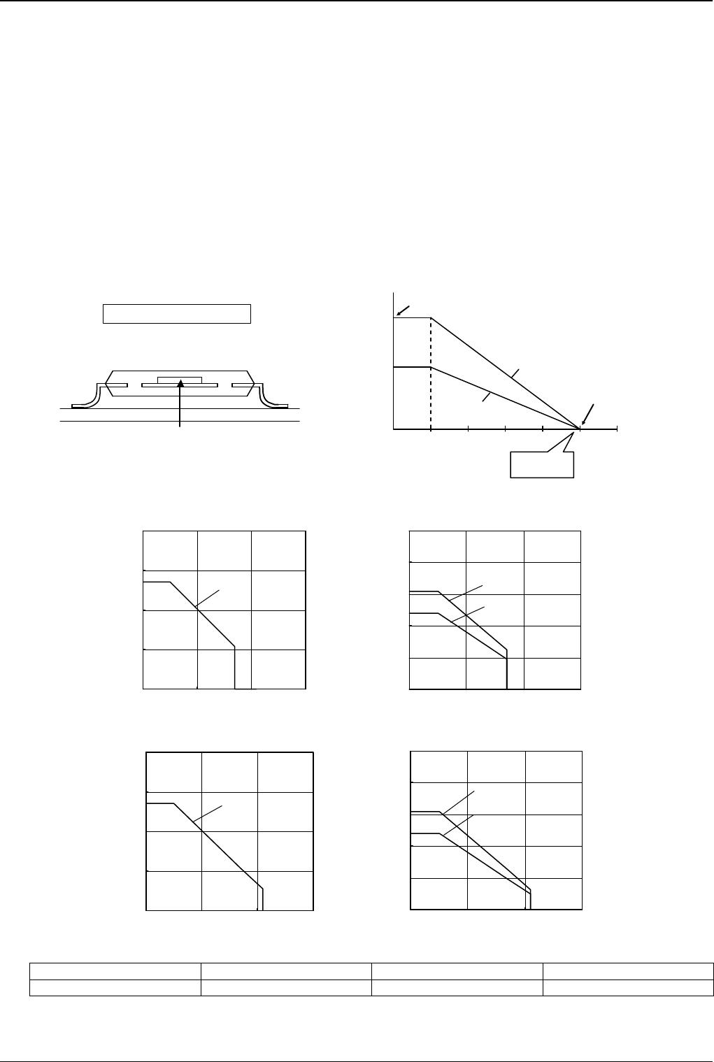
1.4 Power dissipation (Pd)
Indicates the power that can be consumed by specified mounted board at the ambient temperature 25(normal temperature).
As for package product, Pd is determined by the temperature that can be permitted by IC chip in the package(maximum
junction temperature) and thermal resistance of the package
2. Electrical characteristics item
2.1 Input offset voltage (Vio)
Indicates the voltage difference between non-inverting terminal and inverting terminal.
It can be translated into the input voltage difference required for setting the output voltage at 0 [V]
2.2 Input offset current (Iio)
Indicates the difference of input bias current between non-inverting terminal and inverting terminal.
2.3 Input bias current (Ib)
Indicates the current that flows into or out of the input terminal. It is defined by the average of input bias current at
non-inverting terminal and input bias current at inverting terminal.
2.4 Input common-mode voltage range (Vicm)
Indicates the input voltage range where IC operates normally.
2.5 Large signal voltage gain (AV)
Indicates the amplifying rate (gain) of output voltage against the voltage difference between non-inverting terminal and
inverting terminal. It is normally the amplifying rate (gain) with reference to DC voltage.
Av = (Output voltage fluctuation) / (Input offset fluctuation)
2.6 Circuit current (ICC)
Indicates the IC current that flows under specified conditions and no-load steady status.
2.7 Output sink current (OL)
Indicates the maximum current that can be output under specified output condition (such as output voltage and load condition).
2.8 Output saturation voltage, Low level output voltage (VOL)
Indicates the voltage range that can be output under specified load conditions.
2.9 Output leakage current, High level output current(I leak)
Indicates the current that flows into IC under specified input and output conditions.
2.10 Response Time (Tre)
The interval between the application of an input and output condition.
2.11 Common-mode rejection ratio (CMRR)
Indicates the ratio of fluctuation of input offset voltage when in-phase input voltage is changed. It is normally the fluctuation of DC.
CMRR (Change of Input common-mode voltage)/(Input offset fluctuation)
2.12 Power supply rejection ratio (PSRR)
Indicates the ratio of fluctuation of input offset voltage when supply voltage is changed. It is normally the fluctuation of DC.
PSRR(Change of power supply voltage)/(Input offset fluctuation)
Technical Note
BU7251G,BU7251SG, BU7231G,BU7231SG,
BU7252F/FVM,BU7252S F/FVM,BU7232F/FVM,BU7232S F/FVM
15/18
Derating curve
Power dissipation (total loss) indicates the power that can be consumed by IC at Ta=25(normal temperature).IC is heated
when it consumed power, and the temperature of IC ship becomes higher than ambient temperature. The temperature that
can be accepted by IC chip depends on circuit configuration, manufacturing process, and consumable power is limited. Power
dissipation is determined by the temperature allowed in IC chip (maximum junction temperature) and thermal resistance of
package (heat dissipation capability). The maximum junction temperature is typically equal to the maximum value in the
storage package (heat dissipation capability). The maximum junction temperature is typically equal to the maximum value in
the storage temperature range. Heat generated by consumed power of IC radiates from the mold resin or lead frame of the
package. The parameter which indicates this heat dissipation capability (hardness of heat release) is called thermal
resistance, represented by the symbol θj-a[/W]. The temperature of IC inside the package can be estimated by this thermal
resistance. Fig.93 (a) shows the model of thermal resistance of the package. Thermal resistance θja, ambient temperature Ta,
junction temperature Tj, and power dissipation Pd can be calculated by the equation below :
θja (Tj-Ta) / Pd [/W] ・・・・・ ()
Derating curve in Fig.93 (b) indicates power that can be consumed by IC with reference to ambient temperature. Power that
can be consumed by IC begins to attenuate at certain ambient temperature. This gradient is determined by thermal
resistance θja. Thermal resistance θja depends on chip size, power consumption, package, ambient temperature, package
condition, wind velocity, etc even when the same of package is used. Thermal reduction curve indicates a reference value
measured at a specified condition. Fig94(c)-(f) show a derating curve for an example of BU7251family, BU7252 family, BU7231
family, BU7232 family.
(*8) (*9) (*10) Unit
5.4 6.2 4.8 [mW/]
When using the unit above Ta=25[], subtract the value above per degree[]. Permissible dissipation is the value
when FR4 glass epoxy board 70[mm]×70[mm]×1.6[mm] (cooper foil area below 3[%]) is mounted.
Fig. 94.
0507510012515025
P1
P2
Pd(max)
LSI
の消費電力
[W]
θja2
θja1
Tj(max)
θja2 < θja1
周囲温度
Ta[
]
BU7251/BU7231
Tj(max)
Power dissipation Pd:[W]
A
mbient temperature:Ta
[
]
(a) Thermal resistance
(b) Derating curve
Fig. 93. Thermal resistance and power dissipation
Derating curve
0
200
400
600
800
050100150
AMBIENT TEMPERATURE [
]
POWER DISSIPATION [mW]
.
85
0
200
400
600
800
1000
0 50 100 150
AMBIENT TEMPERATURE [
]
POWER DISSIPATION [mW]
.
85
0
200
400
600
800
0 50 100 150
AMBIENT TEMPERATURE [
]
POWER DISSIPATION [mW]
.
BU7231SG(*8)
105
0
200
400
600
800
1000
0 50 100 150
AMBIENT TEMPERATURE [
]
POWER DISSIPATION [mW]
.
105
(c) BU7251G BU7231G
(d) BU7252F/FVM BU7232F/FVM
(e) BU7251SG BU7231SG (f) BU7252S F/FVM BU72432S F/FVM
BU7251SG(*8)
BU7251G(*8)
BU7231G(*8)
540[mw]
620[mw]
480[mw]
540[mw]
BU7252F(*9)
BU7232F(*9)
BU7252FVM(*10)
BU7232FVM(*10)
620[mw]
480[mw]
BU7252SF(*9)
BU7232SF(*9)
BU7252SFVM(*10)
BU7232SFVM(*10)
A
mbient temperature Ta
[
]
Chip surface temperature Tj [
]
Power dissi pa tion P [W]
θja = ( Tj
Ta ) / Pd [
/W]

BU7231G-TR

Mfr. #:
Manufacturer:
Description:
Operational Amplifiers - Op Amps 1.8-5.5V 1 CHAN 0.005mV 0.001nA
Lifecycle:
New from this manufacturer.
Delivery:
DHL FedEx Ups TNT EMS
Payment:
T/T Paypal Visa MoneyGram Western Union