HTMS1x01_8x01 All information provided in this document is subject to legal disclaimers. © NXP Semiconductors N.V. 2015. All rights reserved.
Product data sheet
COMPANY PUBLIC
Rev. 3.4 — 21 May 2015
152934 16 of 57
NXP Semiconductors
HTMS1x01; HTMS8x01
HITAG µ transponder IC
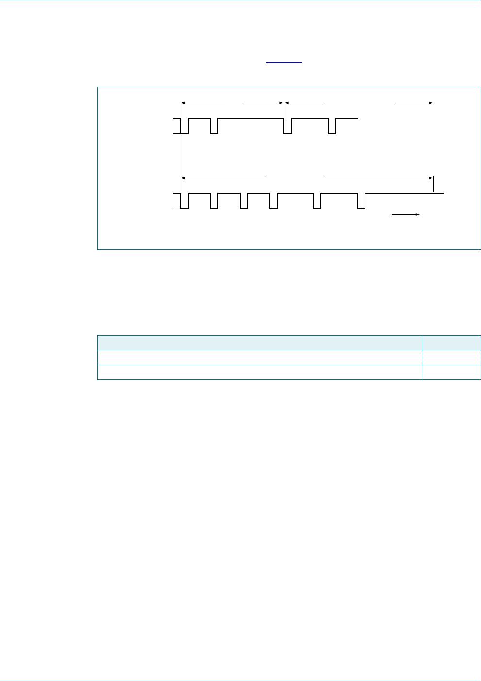
11.2 Mode switching protocol
After powering the HITAG µ transponder IC switches to the data exchange mode after
receiving one of the two possible switch commands from the RWD during the specified
switch window (see Table 10
and Figure 4 for details).
[1] T
C...
Carrier period time (

kHz = 7.45 s nominal)
Fig 4. Switching window timing
Table 10. HITAG µ transponder IC air interface parameters
[1]
Parameter Description
Interrogation field modulation Amplitude modulation (ASK), 90 - 100%
Encoding Pulse Interval Encoding; Least Significant Bit (LSB) first
Bit rate 5.2 kbit/s typically
Mode switching Either a specific 5 bit switch command or the detection of the
SOF as part of a valid
HITAG µ transponder IC command,
transmitted after the interruption of the interrogation field for at
least 5 ms
Mode switch timing
HITAG µ transponder IC settling time: 312.5 T
C
switch
command window after HITAG µ transponder IC settling:
232.5 T
C
All within cycle C in Figure 3.
Mode switch command 00011 or SOF sequence
001aak278
312.5 × T
c
232 × T
c
TTF operation in case
of no command
during switching window
HTMS1x01_8x01 All information provided in this document is subject to legal disclaimers. © NXP Semiconductors N.V. 2015. All rights reserved.
Product data sheet
COMPANY PUBLIC
Rev. 3.4 — 21 May 2015
152934 17 of 57
NXP Semiconductors
HTMS1x01; HTMS8x01
HITAG µ transponder IC
The RWD sends either the SOF at the start of a valid request or a special switch
command to the HITAG µ (as shown in Figure 5
) in order to transfer it into the data
exchange mode.
11.2.1 SWITCH
Setting the transponder into data exchange mode (advanced mode) is done by sending
SOF pattern or the switch command within the listening window (232.5 x T
C
). The
SWITCH command itself does not contain SOF and EOF.
Fig 5. Reader downlink modulation for SWITCH command
001aaj825
carrier on
0
0 0 0 1 1 stop condition
time
code violation
SOF
FDX ADV command
carrier off
transceiver
carrier on
carrier off
0
switch command
Table 11. SWITCH Command
Command Description
5 No. of bits
00011
HTMS1x01_8x01 All information provided in this document is subject to legal disclaimers. © NXP Semiconductors N.V. 2015. All rights reserved.
Product data sheet
COMPANY PUBLIC
Rev. 3.4 — 21 May 2015
152934 18 of 57
NXP Semiconductors
HTMS1x01; HTMS8x01
HITAG µ transponder IC
11.3 Downlink communication signal interface - RWD to HITAG µ
transponder IC
11.3.1 Modulation parameters
Communications between RWD and HITAG µ transponder IC takes place using ASK
modulation with a modulation index of m > 90%.
[1] T
F3
shall not exceed T
Fd0
- T
F1
- 3 T
c
[2] T
C...
Carrier period time (

kHz = 7.45 s nominal)
Fig 6. Modulation details of data transmission from RWD to HITAG µ transponder IC
Table 12. Modulation coding times
[1][2]
Symbol Min Max
m = (a-b)/(a+b) 90% 100%
T
F1
4 T
c
10 T
c
T
F2
00.5 T
F1
T
F3
00.5 T
Fd0
x00.05 a
y00.05 a

HTMS8201FTB/AF,115

Mfr. #:
Manufacturer:
NXP Semiconductors
Description:
RFID Transponders RFID HTAG ADVANCED
Lifecycle:
New from this manufacturer.
Delivery:
DHL FedEx Ups TNT EMS
Payment:
T/T Paypal Visa MoneyGram Western Union