HTMS1x01_8x01 All information provided in this document is subject to legal disclaimers. © NXP Semiconductors N.V. 2015. All rights reserved.
Product data sheet
COMPANY PUBLIC
Rev. 3.4 — 21 May 2015
152934 4 of 57
NXP Semiconductors
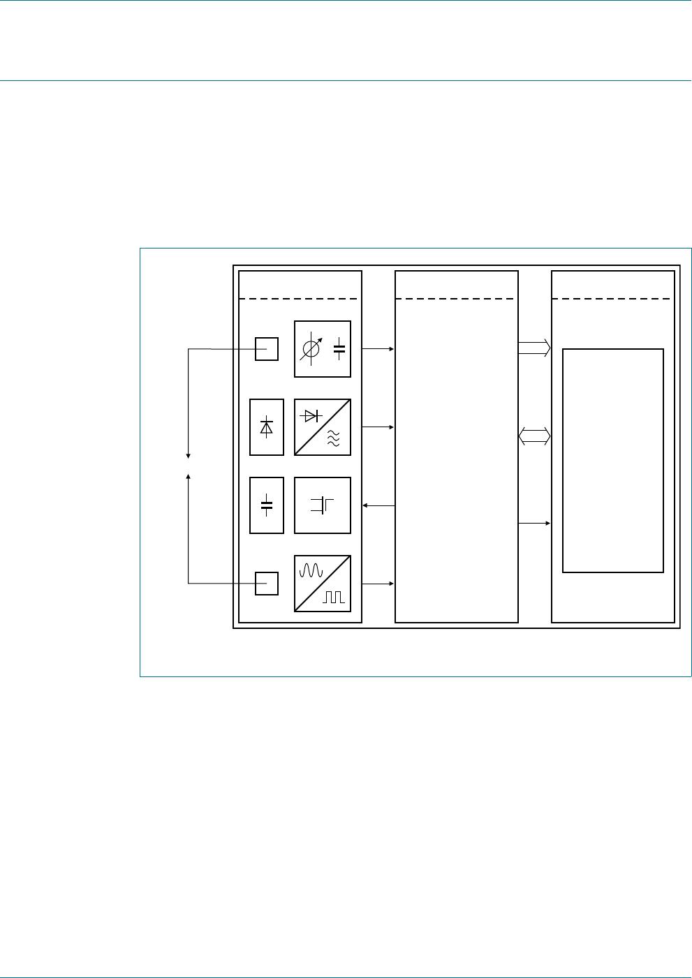
HTMS1x01; HTMS8x01
HITAG µ transponder IC
5. Ordering information
Table 2. Ordering information
Type number Package
Name Description Type Version
HTMS1001FUG/AM Wafer sawn, megabumped wafer, 150 µm, 8 inch, UV HITAG , 210 pF -
HTMS8001FUG/AM Wafer sawn, megabumped wafer, 150 µm, 8 inch, UV HITAG , 280pF -
HTMS8101FUG/AM Wafer sawn, megabumped wafer, 150 µm, 8 inch, UV HITAG Advanced,
280 pF
-
HTMS8201FUG/AM Wafer sawn, megabumped wafer, 150 µm, 8 inch, UV HITAG Advanced+,
280 pF
-
HTMS8001FTB/AF XSON3 plastic extremely thin small outline package; no
leads; 4 terminals; body 1 1.45 0.5 mm
HITAG , 280 pF SOT1122
HTMS8101FTB/AF XSON3 plastic extremely thin small outline package; no
leads; 4 terminals; body 1 1.45 0.5 mm
HITAG Advanced,
280 pF
SOT1122
HTMS8201FTB/AF XSON3 plastic extremely thin small outline package; no
leads; 4 terminals; body 1 1.45 0.5 mm
HITAG Advanced+,
280 pF
SOT1122
HTMS8001FTK/AF HVSON2 plastic thermal enhanced very thin small outline
package; no leads; 2 terminals; body 3 2
0.85 mm
HITAG , 280 pF SOT899-1
HTMS8101FTK/AF HVSON2 plastic thermal enhanced very thin small outline
package; no leads; 2 terminals; body 3 2
0.85 mm
HITAG Advanced,
280 pF
SOT899-1
HTMS8201FTK/AF HVSON2 plastic thermal enhanced very thin small outline
package; no leads; 2 terminals; body 3 2
0.85 mm
HITAG Advanced+,
280 pF
SOT899-1