13
LTC1197/LTC1197L
LTC1199/LTC1199L
1197/99 F02
CLK
CS
t
dDO
t
suCS
B0*
B1B2B3B4
B5
B6B7
B8B9
NULL
BITS
Hi-Z
1413121110987654321 15 16
1
D
OUT
D
IN
HI-Z
START
DUMMY
DON’T CARE
ODD/
SIGN
SGL/
DIFF
*AFTER COMPLETING THE DATA TRANSFER, IF FURTHER CLOCKS ARE APPLIED WITH CS LOW,
THE ADC WILL OUTPUT ZEROS INDEFINITELY
t
en
t
CYC
(16 CLKs)*
t
CONV
(10.5 CLKs)
POWER
DOWN
t
SMPL
(1.5 CLKs)
Figure 2. LTC1199/LTC1199L Operating Sequence
transfer and all leading zeros that precede this logical one
will be ignored. After the start bit is received the remaining
bits of the input word will be clocked in. Further inputs on
the D
IN
pin are then ignored until the next CS cycle.
Multiplexer (MUX) Address
The bits of the input word following the start bit assign the
MUX configuration for the requested conversion. For a
given channel selection, the converter will measure the
voltage between the two channels indicated by the “+” and
“–” signs in the selected row of the following table. In
single-ended mode, all input channels are measured with
respect to GND. Only the + inputs have sample-and-holds.
Signals applied at the – inputs must not change more than
the required accuracy during the conversion.
Multiplexer Channel Selection
MUX ADDRESS
SGL/DIFF
1
1
0
0
ODD/SIGN
0
1
0
1
CHANNEL #
0
+
+
1
+
+
GND
1197/99 AI02
The LTC1197/LTC1197L do not require a configuration
input word and have no D
IN
pin. A falling CS initiates data
transfer as shown in the LTC1197/LTC1197L operating
sequence. After CS falls, the second CLK pulse enables
D
OUT
. After two null bits, the A/D conversion result is output
on the D
OUT
line in MSB-first format. Bringing CS high
resets the LTC1197/LTC1197L for the next data exchange
and minimizes the supply current if CLK is continuously
running.
INPUT DATA WORD (LTC1199/LTC1199L ONLY)
The LTC1199 4-bit data word is clocked into the D
IN
input
on the rising edge of the clock after CS goes low and the
start bit has been recognized. Further inputs on the D
IN
pin
are then ignored until the next CS cycle. The input word is
defined as follows:
SGL/
DIFF
ODD/
SIGN
DUMMYSTART
MUX
ADDRESS
1197/99 AI01
Start Bit
The first “logical one” clocked into the D
IN
input after CS
goes low is the start bit. The start bit initiates the data
APPLICATIO S I FOR ATIO
WUUU
14
LTC1197/LTC1197L
LTC1199/LTC1199L
Dummy Bit
The dummy bit is a placeholder that extends the acquisi-
tion time of the ADC. This bit can be either high or low and
does not affect the conversion of the ADC.
Operation with D
IN
and D
OUT
Tied Together
The LTC1199/LTC1199L can be operated with D
IN
and
D
OUT
tied together. This eliminates one of the lines
required to communicate to the microprocessor (MPU).
Data is transmitted in both directions on a single wire. The
processor pin connected to this data line should be
configurable as either an input or an output. The LTC1199/
LTC1199L will take control of the data line and drive it low
on the 4th falling CLK edge after the start bit is received
(see Figure 3). Therefore the processor port line must be
switched to an input before this happens to avoid a
conflict.
In the Typical Applications section, there is an example of
interfacing the LTC1199/LTC1199L with D
IN
and D
OUT
tied together to the Intel 8051 MPU.
Unipolar Transfer Curve
The LTC1197/LTC1197L/LTC1199/LTC1199L are perma-
nently configured for unipolar only. The input span and
code assignment for this conversion type are shown in the
following figures for a 5V reference.
1
2 3 4
CS
CLK
DATA (D
IN
/D
OUT
) START SGL/DIFF ODD/SIGN DUMMY B9NULL BITS B8
LTC1199/LTC1199L CONTROL DATA LINE
AND SEND A/D RESULT BACK TO MPU
MPU CONTROLS DATA LINE AND SENDS
MUX ADDRESS TO LTC1199/LTC1199L
PROCESSOR MUST RELEASE
DATA LINE AFTER 4TH RISING CLK
AND BEFORE THE 4TH FALLING CLK
LTC1199/LTC1199L TAKE CONTROL OF
DATA LINE ON 4TH FALLING CLK
1197/99 F03
Figure 3. LTC1199/LTC1199L Operation with D
IN
and D
OUT
Tied Together
Unipolar Transfer Curve
0V
1LSB
V
REF
– 2LSB
V
REF
– 1LSB
V
REF
V
IN
0 0 0 0 0 0 0 0 0 1
0 0 0 0 0 0 0 0 0 0
1 1 1 1 1 1 1 1 1 1
1 1 1 1 1 1 1 1 1 0
1197/99 AI03
Unipolar Output Code
OUTPUT CODE
1 1 1 1 1 1 1 1 1 1
1 1 1 1 1 1 1 1 1 0
0 0 0 0 0 0 0 0 0 1
0 0 0 0 0 0 0 0 0 0
INPUT VOLTAGE
V
REF
– 1LSB
V
REF
– 2LSB
1LSB
0V
INPUT VOLTAGE
(V
REF
= 5.000V)
4.99512V
4.99023V
4.88mV
0V
1197/99 AI04
ACHIEVING MICROPOWER PERFORMANCE
With typical operating currents of 5mA (LTC1197/
LTC1199) at 5V and 0.8mA (LTC1197L/LTC1199L) at
2.7V it is possible for these ADCs to achieve true
micropower performance by taking advantage of the
automatic shutdown between conversions. In systems
APPLICATIO S I FOR ATIO
WUUU
15
LTC1197/LTC1197L
LTC1199/LTC1199L
Lower Supply Voltage
For lower supply voltages, LTC offers the LTC1197L/
LTC1199L. These pin compatible devices offer specified
performance to 2.7V supplies.
OPERATING ON OTHER THAN 5V SUPPLIES
The LTC1197 operates from 4V to 9V supplies and the
LTC1199 operates from 4V to 6V supplies. The LTC1197L/
LTC1199L operate from 2.7V to 4V supplies. To use these
parts at other than 5V supplies a few things must be kept
in mind.
Bypassing
At higher supply voltages, bypass capacitors on V
CC
and
V
REF
if applicable, need to be increased beyond what is
necessary for 5V. For a 9V supply a 10µF tantalum in
parallel with a 0.1µF ceramic is recommended.
Input Logic Levels
The input logic levels of CS, CLK and D
IN
are made to meet
TTL threshold levels on a 5V supply. When the supply
voltage varies, the input logic levels also change. For the
ADC to sample and convert correctly, the digital inputs
have to meet logic low and high levels relative to the
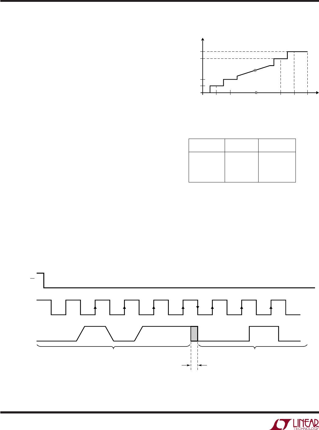
operating supply voltage (see typical curve of Digital Input
Logic Threshold vs Supply Voltage). If achieving mi-
cropower consumption is desirable, the digital inputs
must go rail-to-rail between V
CC
and ground (see ACHIEV-
ING MICROPOWER PERFORMANCE section).
Clock Frequency
The maximum recommended clock frequency is 7.2MHz
for the LTC1197/LTC1199 running off a 5V supply and
3.5MHz for the LTC1197L/LTC1199L running off a 2.7V
supply. With the supply voltage changing, the maximum
clock frequency for the devices also changes (see the
typical curve of Maximum Clock Rate vs Supply Voltage).
If the maximum clock frequency is used, care must be
taken to ensure that the device converts correctly.
that convert continuously, the LTC1197/LTC1197L/
LTC1199/LTC1199L will draw their normal operating power
continuously. Several things must be taken into account
to achieve micropower operation.
Shutdown
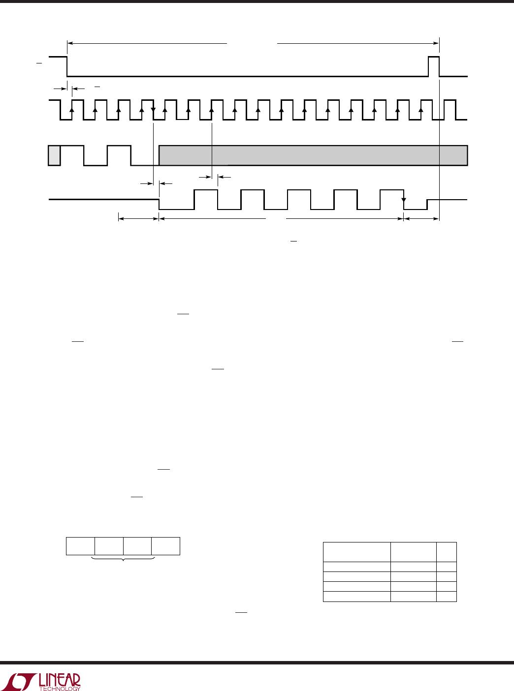
Figures 1 and 2 show the operating sequence of the
LTC1197/LTC1197L/LTC1199/LTC1199L. The converter
draws power when the CS pin is low and powers itself
down when that pin is high. If the CS pin is not taken all the
way to ground when it is low and not taken to V
CC
when it
is high, the input buffers of the converter will draw current.
This current may be tens of microamps. It is worthwhile to
bring the CS pin all the way to ground when it is low and
all the way to V
CC
when it is high to obtain the lowest
supply current.
When the CS pin is high (= supply voltage), the converter
is in shutdown mode and draws only leakage current. The
status of the D
IN
and CLK inputs have no effect on supply
current during this time. There is no need to stop D
IN
and
CLK with CS = high, except the MPU may benefit.
Minimize CS Low Time
In systems that have significant time between conver-
sions, lowest power drain will occur with the minimum CS
low time. Bringing CS low, transferring data as quickly as
possible, and then returning CS high will result in the
lowest possible current drain. This minimizes the amount
of time the device draws power. Even though the device
draws more power at high clock rates, the net power is less
because the device is on for a shorter time.
D
OUT
Loading
Capacitive loading on the digital output can increase
power consumption. A 100pF capacitor on the D
OUT
pin
can add 200µA to the supply current at a 7.2MHz clock
frequency. The extra 200µA goes into charging and dis-
charging the load capacitor. The same goes for digital lines
driven at a high frequency by any logic. The C V • f currents
must be evaluated and the troublesome ones minimized.
APPLICATIO S I FOR ATIO
WUUU

LTC1197LCMS8#TRPBF

Mfr. #:
Manufacturer:
Analog Devices Inc.
Description:
Analog to Digital Converters - ADC 250ksps Diff input 3V 10-Bit ADC
Lifecycle:
New from this manufacturer.
Delivery:
DHL FedEx Ups TNT EMS
Payment:
T/T Paypal Visa MoneyGram Western Union