16
LTC1197/LTC1197L
LTC1199/LTC1199L
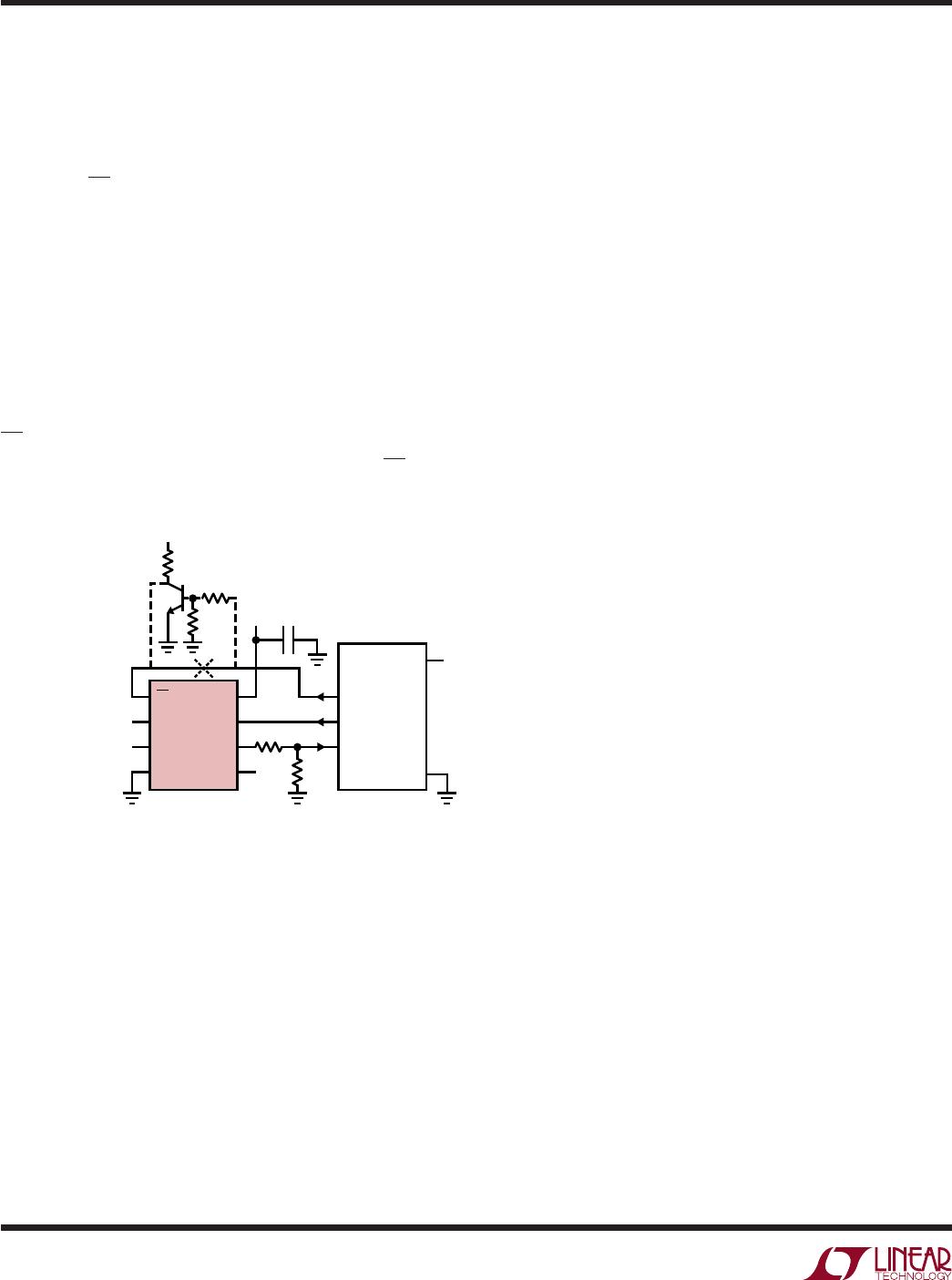
Mixed Supplies
It is possible to have a microprocessor running off a 5V
supply and communicate with the ADC operating on 3V or
9V supplies. The requirement to achieve this is that the
outputs of CS, CLK and D
IN
from the MPU have to be able
to trip the equivalent inputs of the ADC and the output of
the ADC must be able to toggle the equivalent input of the
MPU (see typical curve of Digital Input Logic Threshold vs
Supply Voltage). With the LTC1197 operating on a 9V
supply, the output of D
OUT
may go between 0V and 9V. The
9V output may damage the MPU running off a 5V supply.
The way to solve this problem is to have a resistor divider
on D
OUT
(Figure 4) and connect the center point to the
MPU input. It should be noted that to get full shutdown, the
CS input of the ADC must be driven to the V
CC
voltage. This
would require adding a level shift circuit to the CS signal
in Figure 4.
SAMPLE-AND-HOLD
The LTC1197/LTC1197L/LTC1199/LTC1199L provide a
built-in sample-and-hold (S/H) function to acquire sig-
nals. The S/H of the LTC1197/LTC1197L acquires input
signals for the “+” input relative to the “–” input during the
t
SMPL
time (see Figure 1). However the S /H of the LTC1199/
LTC1199L can sample input signals from the “+” input
relative to ground and from the “–” input relative to ground
in addition to acquiring signals from the “+” input relative
to the “–” input (see Figure 5) during t
SMPL
.
Single-Ended Inputs
The sample-and-hold of the LTC1199/LTC1199L allows
conversion of rapidly varying signals. The input voltage is
sampled during the t
SMPL
time as shown in Figure 5. The
sampling interval begins as the ODD/SGN bit is shifted in
and continues until the falling CLK edge after the dummy
bit is received. On this falling edge, the S/H goes into hold
mode and the conversion begins.
Differential Inputs
With differential inputs, the ADC no longer converts just a
single voltage but rather the difference between two volt-
ages. In this case, the voltage on the selected “+” input is
still sampled and held and therefore may be rapidly time
varying just as in single-ended mode. However, the volt-
age on the selected “–” input must remain constant and be
free of noise and ripple throughout the conversion time.
Otherwise, the differencing operation may not be per-
formed accurately. The conversion time is 10.5 CLK cycles.
Therefore, a change in the “–” input voltage during this
interval can cause conversion errors. For a sinusoidal
voltage on the “–” input this error would be:
V
ERROR (MAX)
= V
PEAK
• 2 • π • f(“–”) • 10.5/f
CLK
Where f(“–”) is the frequency of the “–” input voltage,
V
PEAK
is its peak amplitude and f
CLK
is the frequency of the
CLK. In most cases V
ERROR
will not be significant. For a
60Hz signal on the “–” input to generate a 1/4LSB error
(1.22mV) with the converter running at CLK = 7.2MHz, its
peak value would have to be 2.22V.
Figure 4. Interfacing a 9V-Powered LTC1197 to a 5V System
BOARD LAYOUT CONSIDERATIONS
Grounding and Bypassing
The LTC1197/LTC1197L/LTC1199/LTC1199L should be
used with an analog ground plane and single point ground-
ing techniques. The GND pin should be tied directly to the
ground plane. The V
CC
pin should be bypassed to the
ground plane using a 1µF tantalum capacitor with leads as
short as possible. All analog inputs should be referenced
directly to the single point ground. Digital inputs and
outputs should be shielded from and/or routed away from
the reference and analog circuitry.
APPLICATIO S I FOR ATIO
WUUU
+IN
–IN
GND
V
CC
CLK
D
OUT
V
REF
4.7k
4.7k6V
4.7µF
MPU
(e.g. 8051)
5V
P1.4
P1.3
P1.2
1197/99 F04
DIFFERENTIAL INPUTS
COMMON MODE RANGE
0V TO 6V
9V
LTC1197
9V
OPTIONAL
LEVEL SHIFT
CS