74CBTLV3125 All information provided in this document is subject to legal disclaimers. © NXP Semiconductors N.V. 2016. All rights reserved.
Product data sheet Rev. 4 — 9 November 2016 9 of 18
NXP Semiconductors
74CBTLV3125
4-bit bus switch
11. Waveforms
Measurement points are given in Table 9.
Logic levels: V
OL
and V
OH
are typical output voltage levels that occur with the output load.
Fig 15. The data input (nA or nB) to output (nB or nA) propagation delays
DDL
9
0
9
0
9
0
9
0
9
,
LQSXW
9
9
2+
RXWSXW
9
2/
W
3+/
W
3/+
Table 9. Measurement points
Supply voltage Input Output
V
CC
V
M
V
I
t
r
= t
f
V
M
V
X
V
Y
2.3 V to 2.7 V 0.5V
CC
V
CC
2.0 ns 0.5V
CC
V
OL
+0.15V V
OH
0.15 V
3.0 V to 3.6 V 0.5V
CC
V
CC
2.0 ns 0.5V
CC
V
OL
+0.3V V
OH
0.3 V
Measurement points are given in Table 9.
Logic levels: V
OL
and V
OH
are typical output voltage levels that occur with the output load.
Fig 16. Enable and disable times
9
,
9
2/
9
2+
*1'
Q2(LQSXW
RXWSXW
/2:WR2))
2))WR/2:
RXWSXW
+,*+WR2))
2))WR+,*+
*1'
VZLWFK
HQDEOHG
VZLWFK
HQDEOHG
DDN
VZLWFK
GLVDEOHG
9
&&
9
0
9
0
9
0
9
;
9
<
W
3/=
W
3+=
W
3=+
W
3=/
74CBTLV3125 All information provided in this document is subject to legal disclaimers. © NXP Semiconductors N.V. 2016. All rights reserved.
Product data sheet Rev. 4 — 9 November 2016 10 of 18
NXP Semiconductors
74CBTLV3125
4-bit bus switch
Test data is given in Table 10.
Definitions for test circuit:
R
L
= Load resistance.
C
L
= Load capacitance including jig and probe capacitance.
R
T
= Termination resistance should be equal to the output impedance Z
o
of the pulse generator.
V
EXT
= External voltage for measuring switching times.
Fig 17. Test circuit for measuring switching times
9
0
9
0
W
:
W
:


9
9
,
9
,
QHJDWLYH
SXOVH
SRVLWLYH
SXOVH
9
9
0
9
0


W
I
W
U
W
U
W
I
DDH
9
(;7
9
&&
9
,
9
2
'87
&
/
5
7
5
/
5
/
*
Table 10. Test data
Supply voltage Load V
EXT
V
CC
C
L
R
L
t
PLH
, t
PHL
t
PZH
, t
PHZ
t
PZL
, t
PLZ
2.3 V to 2.7 V 30 pF 500 open GND 2V
CC
3.0 V to 3.6 V 50 pF 500 open GND 2V
CC
74CBTLV3125 All information provided in this document is subject to legal disclaimers. © NXP Semiconductors N.V. 2016. All rights reserved.
Product data sheet Rev. 4 — 9 November 2016 11 of 18
NXP Semiconductors
74CBTLV3125
4-bit bus switch
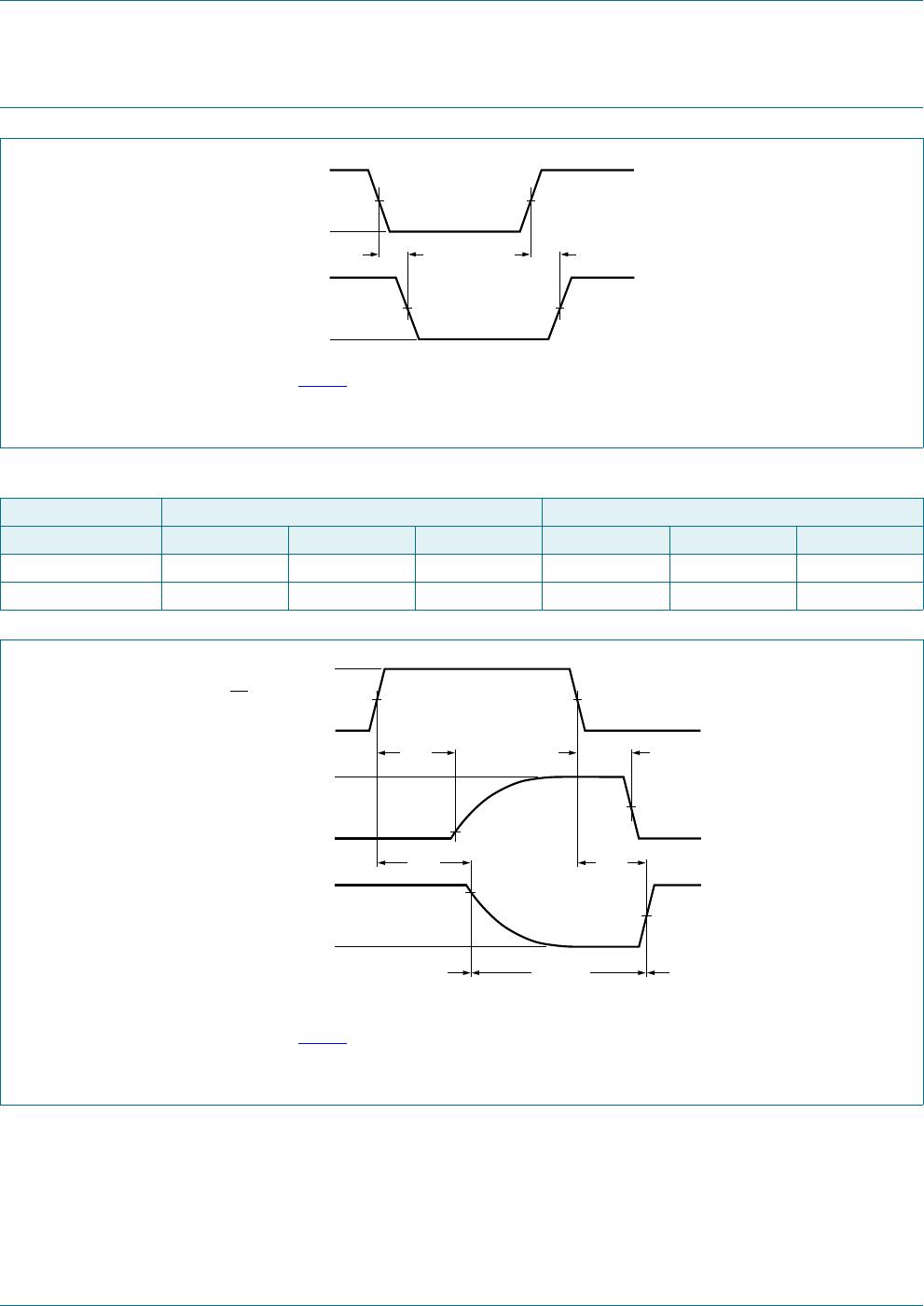
11.1 Additional dynamic characteristics
[1] f
i
is biased at 0.5V
CC
.
11.2 Test circuit
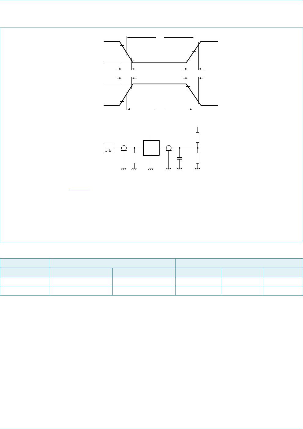
Table 11. Additional dynamic characteristics
At recommended operating conditions; voltages are referenced to GND (ground = 0 V); V
I
= GND or V
CC
(unless otherwise
specified); t
r
= t
f

2.5 ns.
Symbol Parameter Conditions T
amb
= 25 C Unit
Min Typ Max
f
(3dB)
3 dB frequency response V
CC
=3.3V; R
L
=50; see Figure 18
[1]
-406-MHz
nOE connected to GND; Adjust f
i
voltage to obtain 0 dBm level at output. Increase f
i
frequency until dB meter reads 3dB.
Fig 18. Test circuit for measuring the frequency response when channel is in ON-state
DDD
9
&&
9
,/
I
L
9
&&
5
/
*1'
G%
Q2(
Q$
Q%

74CBTLV3125PW,118

Mfr. #:
Manufacturer:
Nexperia
Description:
Digital Bus Switch ICs Single 60Ohms 3.6V
Lifecycle:
New from this manufacturer.
Delivery:
DHL FedEx Ups TNT EMS
Payment:
T/T Paypal Visa MoneyGram Western Union

Products related to this Datasheet