74CBTLV3125 All information provided in this document is subject to legal disclaimers. © NXP Semiconductors N.V. 2016. All rights reserved.
Product data sheet Rev. 4 — 9 November 2016 8 of 18
NXP Semiconductors
74CBTLV3125
4-bit bus switch
10. Dynamic characteristics
[1] All typical values are measured at T
amb
=25C and at nominal V
CC
.
[2] The propagation delay is the calculated RC time constant of the typical on-state resistance of the switch and the load capacitance, when
driven by an ideal voltage source (zero output impedance).
[3] t
pd
is the same as t
PLH
and t
PHL
.
[4] t
en
is the same as t
PZH
and t
PZL
.
[5] t
dis
is the same as t
PHZ
and t
PLZ
.
(1) T
amb
= 125 C.
(2) T
amb
= 85 C.
(3) T
amb
= 25 C.
(4) T
amb
= 40 C.
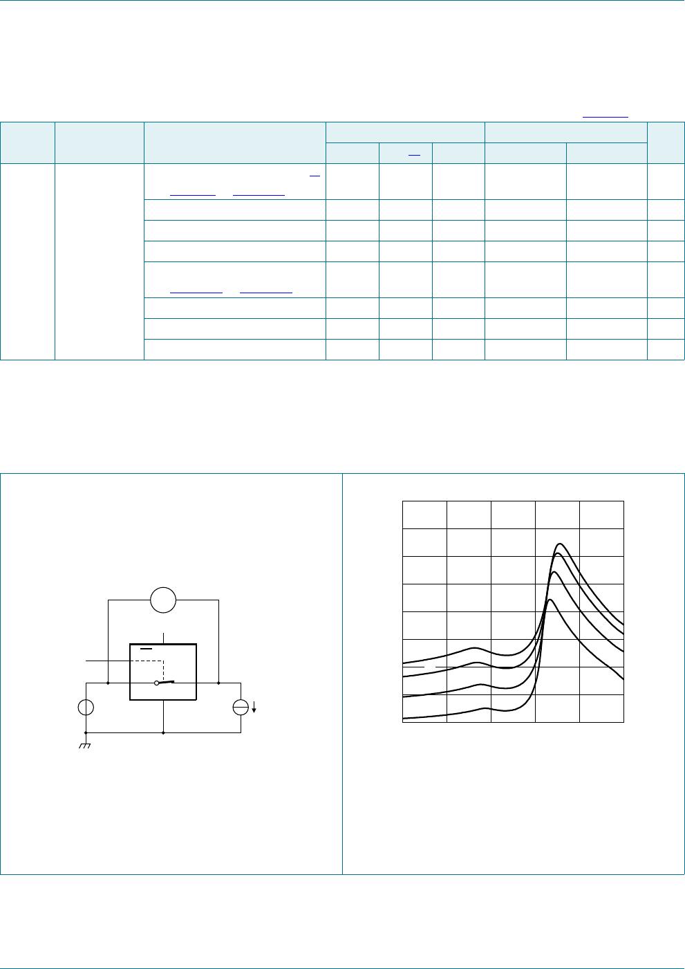
Fig 14. ON resistance as a function of input voltage; V
CC
= 3.3 V; I
SW
= 64 mA
9
,
9
DDL
5
21
ȍ
Table 8. Dynamic characteristics
GND = 0 V; for test circuit see Figure 17
Symbol Parameter Conditions T
amb
= 40 C to +85 C T
amb
= 40 C to +125 C Unit
Min Typ
[1]
Max Min Max
t
pd
propagation delay nA to nB or nB to nA;
see Figure 15
[2][3]
V
CC
= 2.3 V to 2.7 V - - 0.13 - 0.20 ns
V
CC
= 3.0 V to 3.6 V - - 0.20 - 0.31 ns
t
en
enable time nOE to nA or nB;
see Figure 16
[4]
V
CC
= 2.3 V to 2.7 V 1.0 2.7 4.6 1.0 6.0 ns
V
CC
= 3.0 V to 3.6 V 1.0 2.4 4.4 1.0 6.0 ns
t
dis
disable time nOE to nA or nB;
see Figure 16
[5]
V
CC
= 2.3 V to 2.7 V 1.0 2.2 3.9 1.0 5.5 ns
V
CC
= 3.0 V to 3.6 V 1.0 2.9 4.2 1.0 5.5 ns