74CBTLV3125 All information provided in this document is subject to legal disclaimers. © NXP Semiconductors N.V. 2016. All rights reserved.
Product data sheet Rev. 4 — 9 November 2016 4 of 18
NXP Semiconductors
74CBTLV3125
4-bit bus switch
7. Limiting values
[1] The minimum input voltage rating may be exceeded if the input clamping current ratings are observed.
[2] The switch voltage ratings may be exceeded if switch clamping current ratings are observed
[3] For SSOP16 and TSSOP14 packages: P
tot
derates linearly with 5.5 mW/K above 60 C.
For DHVQFN14 packages: P
tot
derates linearly with 4.5 mW/K above 60 C.
8. Recommended operating conditions
9. Static characteristics
Table 4. Limiting values
In accordance with the Absolute Maximum Rating System (IEC 60134). Voltages are referenced to GND (ground = 0 V).
Symbol Parameter Conditions Min Max Unit
V
CC
supply voltage 0.5 +4.6 V
V
I
input voltage control inputs
[1]
0.5 +4.6 V
V
SW
switch voltage enable and disable mode
[2]
0.5 V
CC
+ 0.5 V
I
IK
input clamping current V
I
< 0.5 V 50 - mA
I
SK
switch clamping current V
I
< 0.5 V 50 - mA
I
SW
switch current V
SW
= 0 V to V
CC
- 128 mA
I
CC
supply current - +100 mA
I
GND
ground current 100 - mA
T
stg
storage temperature 65 +150 C
P
tot
total power dissipation T
amb
= 40 Cto+125C
[3]
- 500 mW
Table 5. Recommended operating conditions
Symbol Parameter Conditions Min Max Unit
V
CC
supply voltage 2.3 3.6 V
V
I
input voltage control inputs 0 3.6 V
V
SW
switch voltage enable and disable mode 0 V
CC
V
T
amb
ambient temperature 40 +125 C
t/V input transition rise and fall rate pin nOE
; V
CC
= 2.3 V to 3.6 V 0 200 ns/V
Table 6. Static characteristics
At recommended operating conditions voltages are referenced to GND (ground = 0 V).
Symbol Parameter Conditions T
amb
= 40 C to +85 C T
amb
= 40 C to +125 C Unit
Min Typ
[1]
Max Min Max
V
IH
HIGH-level
input voltage
V
CC
= 2.3 V to 2.7 V 1.7 - - 1.7 - V
V
CC
= 3.0 V to 3.6 V 2.0 - - 2.0 - V
V
IL
LOW-level input
voltage
V
CC
= 2.3 V to 2.7 V - - 0.7 - 0.7 V
V
CC
= 3.0 V to 3.6 V - - 0.9 - 0.9 V
I
I
input leakage
current
pin nOE; V
I
= GND to V
CC
;
V
CC
=3.6V
--1.0 - 20 A
I
S(OFF)
OFF-state
leakage current
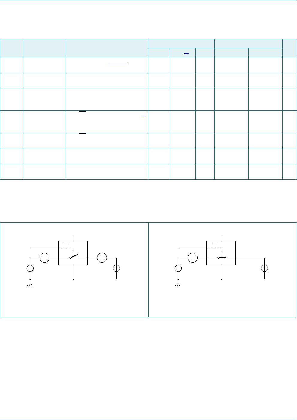
V
CC
= 3.6 V; see Figure 6 --1- 20 A