General Description
The MAX1452 is a highly integrated analog-sensor sig-
nal processor optimized for industrial and process con-
trol applications utilizing resistive element sensors. The
MAX1452 provides amplification, calibration, and tem-
perature compensation that enables an overall perfor-
mance approaching the inherent repeatability of the
sensor. The fully analog signal path introduces no quan-
tization noise in the output signal while enabling digitally
controlled trimming with the integrated 16-bit DACs.
Offset and span are calibrated using 16-bit DACs,
allowing sensor products to be truly interchangeable.
The MAX1452 architecture includes a programmable
sensor excitation, a 16-step programmable-gain ampli-
fier (PGA), a 768-byte (6144 bits) internal EEPROM,
four 16-bit DACs, an uncommitted op amp, and an on-
chip temperature sensor. In addition to offset and span
compensation, the MAX1452 provides a unique tem-
perature compensation strategy for offset TC and
FSOTC that was developed to provide a remarkable
degree of flexibility while minimizing testing costs.
The MAX1452 is packaged for the commercial, industri-
al, and automotive temperature ranges in 16-pin SSOP/
TSSOP and 24-pin TQFN packages.
Customization
Maxim can customize the MAX1452 for high-volume
dedicated applications. Using our dedicated cell library
of more than 2000 sensor-specific functional blocks,
Maxim can quickly provide a modified MAX1452 solu-
tion. Contact Maxim for further information.
Applications
Pressure Sensors
Transducers and Transmitters
Strain Gauges
Pressure Calibrators and Controllers
Resistive Elements Sensors
Accelerometers
Humidity Sensors
Outputs Supported
4–20mA
0 to +5V (rail-to-rail)
+0.5V to +4.5V Ratiometric
+2.5V to ±2.5V
Features
Provides Amplification, Calibration, and
Temperature Compensation
Accommodates Sensor Output Sensitivities
from 4mV/V to 60mV/V
Single Pin Digital Programming
No External Trim Components Required
16-Bit Offset and Span Calibration Resolution
Fully Analog Signal Path
On-Chip Lookup Table Supports Multipoint
Calibration Temperature Correction
Supports Both Current and Voltage Bridge
Excitation
Fast 150µs Step Response
On-Chip Uncommitted Op Amp
Secure-Lock™ Prevents Data Corruption
Low 2mA Current Consumption
Secure-Lock is a trademark of Maxim Integrated Products, Inc.
PART TEMP RANGE PIN-PACKAGE
MAX1452CAE+ 0°C to +70°C 16 SSOP
MAX1452EAE+ -40°C to +85°C 16 SSOP
MAX1452AAE+ -40°C to +125°C 16 SSOP
MAX1452AUE+ -40°C to +125°C 16 TSSOP
MAX1452ATG+ -40°C to +125°C 24 TQFN-EP*
MAX1452C/D 0°C to +70°C Dice**
MAX1452
Low-Cost Precision Sensor
Signal Conditioner
________________________________________________________________
Maxim Integrated Products
1
19-1829; Rev 2; 4/09
EVALUATION KIT
AVAILABLE
For pricing, delivery, and ordering information, please contact Maxim Direct at 1-888-629-4642,
or visit Maxim’s website at www.maxim-ic.com.
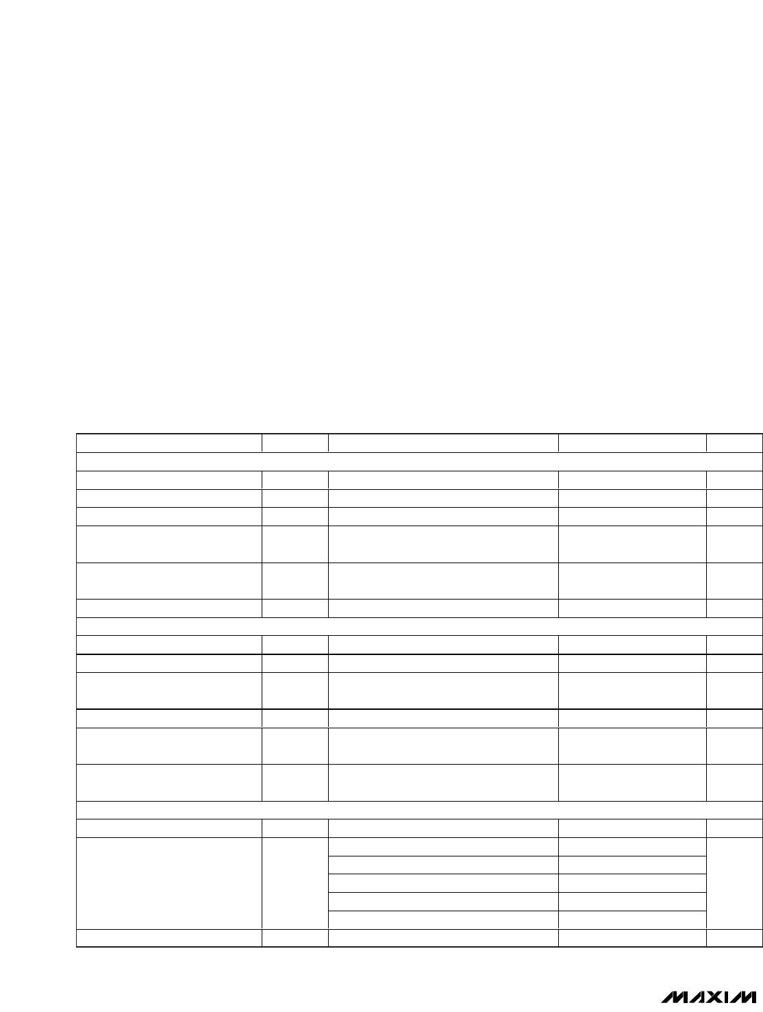
Ordering Information
+
Denotes a lead(Pb)-free/RoHS-compliant package.
*
EP = Exposed pad.
**
Dice are tested at T
A
= +25°C, DC parameters only.
Detailed Block Diagram and Pin Configurations appear at
the end of data sheet.
MAX1452
Low-Cost Precision Sensor
Signal Conditioner
2 _______________________________________________________________________________________
ABSOLUTE MAXIMUM RATINGS
ELECTRICAL CHARACTERISTICS
(V
DD
= V
DDF
= +5V, V
SS
= 0V, T
A
= +25°C, unless otherwise noted.)
Stresses beyond those listed under “Absolute Maximum Ratings” may cause permanent damage to the device. These are stress ratings only, and functional
operation of the device at these or any other conditions beyond those indicated in the operational sections of the specifications is not implied. Exposure to
absolute maximum rating conditions for extended periods may affect device reliability.
Supply Voltage, V
DD
to V
SS
.........................................-0.3V, +6V
Supply Voltage, V
DD
to V
DDF
................................-0.5V to +0.5V
All Other Pins ...................................(V
SS
- 0.3V) to (V
DD
+ 0.3V)
Short-Circuit Duration, FSOTC, OUT, BDR,
AMPOUT ................................................................Continuous
Continuous Power Dissipation (T
A
= +70°C)
16-Pin SSOP/TSSOP (derate 8.00mW/°C above +70°C) ..640mW
24-Pin TQFN (derate 20.8mW/°C above +70°C) ...........1.67W
Operating Temperature:
MAX1452CAE+/MAX1452C/D ............................0°C to +70°C
MAX1452EAE+ ................................................-40°C to +85°C
MAX1452AAE+..............................................-40°C to +125°C
MAX1452AUE+..............................................-40°C to +125°C
MAX1452ATG+..............................................-40°C to +125°C
Junction Temperature......................................................+150°C
Storage Temperature Range .............................-65°C to +150°C
Lead Temperature (soldering, 10s) ................................ +300°C
PARAMETER SYMBOL CONDITIONS MIN TYP MAX UNITS
GENERAL CHARACTERISTICS
Supply Voltage V
DD
4.5 5.0 5.5 V
EEPROM Supply Voltage V
DDF
4.5 5.0 5.5 V
Supply Current I
DD
(Note 1) 2.0 2.5 mA
Maximum EEPROM Erase/Write
Current
I
DDFW
30 mA
Maximum EEPROM Read
Current
I
DDFR
12 mA
Oscillator Frequency f
OSC
0.85 1 1.15 MHz
ANALOG INPUT
Input Impedance R
IN
1MΩ
Input Referred Offset Tempco (Notes 2, 3) ±1 µV/°C
Input Referred Adjustable
Offset Range
Offset TC = 0 at minimum gain (Note 4) ±150 mV
Amplifier Gain Nonlinearity P er cent of + 4V sp an, V
OU T
= + 0.5V to 4.5V 0.01 %
Common-Mode Rejection Ratio CMRR
Specified for common-mode voltages
between V
SS
and V
DD
(Note 2)
90 dB
Input Referred Adjustable
FSO Range
(Note 5) 4 to 60 mV/V
ANALOG OUTPUT
Differential Signal-Gain Range Selectable in 16 steps 39 to 234 V/V
Configuration [5:2] 0000bin 34 39 46
Configuration [5:2] 0001bin 47 52 59
Configuration [5:2] 0010bin 58 65 74
Configuration [5:2] 0100bin 82 91 102
Differential Signal Gain
Configuration [5:2] 1000bin 133 143 157
V/V
Maximum Output-Voltage Swing No load from each supply 0.02 V
MAX1452
Low-Cost Precision Sensor
Signal Conditioner
_______________________________________________________________________________________ 3
ELECTRICAL CHARACTERISTICS (continued)
(V
DD
= V
DDF
= +5V, V
SS
= 0V, T
A
= +25°C, unless otherwise noted.)
PARAMETER SYMBOL CONDITIONS MIN TYP MAX UNITS
Output-Voltage Low I
OUT
= 1mA sinking, T
A
= T
MIN
to T
MAX
0.100 0.20 V
Output-Voltage High I
OU T
= 1m A sour ci ng , T
A
= T
M IN
to T
M AX
4.75 4.87 V
Output Impedance at DC 0.1 Ω
Output Offset Ratio
ΔV
OUT
/
ΔOffset
0.90 1.05 1.20 V/V
Output Offset TC Ratio
Δ V
OU T
/
Δ Offset TC
0.9 1 1.2 V/V
Step Response and IC
(63% Final Value)
150 µs
Maximum Capacitive Load F
Output Noise
DC to 1kHz (gain = minimum, source
impedance = 5kΩ V
DDF
filter)
0.5 m V
RMS
BRIDGE DRIVE
Bridge Current I
BDR
R
L
= 1.7kΩ 0.1 0.5 2 mA
Current Mirror Ratio AA R
ISOURCE
= internal 10 12 14 A/A
V
SPAN
Range (Span Code) T
A
= T
MIN
to T
MAX
4000 C000 hex
DIGITAL-TO-ANALOG CONVERTERS
DAC Resolution 16 Bits
ODAC Bit Weight
ΔV
OUT
/
ΔCode
DAC reference = V
DD
= +5.0V 76 µV/bit
OTCDAC Bit Weight
ΔV
OUT
/
ΔCode
DAC reference = V
BDR
= +2.5V 38 µV/bit
FSODAC Bit Weight
ΔV
OUT
/
ΔCode
DAC reference = V
DD
= +5.0V 76 µV/bit
FSOTCDAC Bit Weight
ΔV
OUT
/
ΔCode
DAC reference = V
BDR
= +2.5V 38 µV/bit
COARSE OFFSET DAC
IRODAC Resolution Including sign 4 Bits
IRODAC Bit Weight
ΔV
OUT
/
ΔCode
Input referred, DAC reference =
V
DD
= +5.0V (Note 6)
9 mV/bit
FSOTC BUFFER
Minimum Output-Voltage Swing No load
V
SS
+
0.1
V
Maximum Output-Voltage Swing No load V
D D
- 1.0 V
Current Drive V
FSOTC
= +2.5V -40 +40 µA
INTERNAL RESISTORS
Current-Source Reference
Resistor
R
ISRC
75 kΩ

MAX1452ATG+T

Mfr. #:
Manufacturer:
Maxim Integrated
Description:
Sensor Interface LO-COST PREC SNSR SIGNAL CDTNR
Lifecycle:
New from this manufacturer.
Delivery:
DHL FedEx Ups TNT EMS
Payment:
T/T Paypal Visa MoneyGram Western Union