MAX1452
Low-Cost Precision Sensor
Signal Conditioner
4 _______________________________________________________________________________________
Note 1: Excludes sensor or load current.
Note 2: All electronics temperature errors are compensated together with sensors errors.
Note 3: The sensor and the MAX1452 must be at the same temperature during calibration and use.
Note 4: This is the maximum allowable sensor offset.
Note 5: This is the sensor's sensitivity normalized to its drive voltage, assuming a desired full span output of +4V and a bridge volt-
age range of +1.7V to +4.25V.
Note 6: Bit weight is ratiometric to V
DD
.
Note 7: Programming of the EEPROM at room temperature is recommended.
Note 8: Allow a minimum of 6ms elapsed time before sending any command.
ELECTRICAL CHARACTERISTICS (continued)
(V
DD
= V
DDF
= +5V, V
SS
= 0V, T
A
= +25°C, unless otherwise noted.)
PARAMETER SYMBOL CONDITIONS MIN TYP MAX UNITS
C ur r ent- S our ce Refer ence
Resi stor Tem p er atur e C oeffi ci ent
Δ R
IS RC
1300 p p m/°C
FSOTC Resistor R
FTC
75 kΩ
FSOTC Resistor Tem p er atur e
C oeffi ci ent
ΔR
FTC
1300 p p m/°C
TEMPERATURE-TO-DIGITAL CONVERTER
Temperature ADC Resolution 8 Bits
Offset ±3 LSB
Gain 1.45 °C/bit
Nonlinearity ±0.5 LSB
Lowest Digital Output 00 hex
Highest Digital Output AF hex
UNCOMMITTED OP AMP
Open-Loop Gain R
L
= 100kΩ 90 dB
Input Common-Mode Range V
SS
V
DD
V
Output Swing No load, T
A
= T
MIN
to T
MAX
V
SS
+
0.02
V
DD
-
0.02
V
Output-Voltage High 1mA source, T
A
= T
MIN
to T
MAX
4.85 4.90 V
Output-Voltage Low 1mA sink, T
A
= T
MIN
to T
MAX
0.05 0.15 V
Offset V
IN+
= +2.5V, unity gain buffer -20 +20 mV
Unity Gain Bandwidth 2 MHz
EEPROM
Maximum Erase/Write Cycles (Note 7) 10k Cycles
Minimum Erase Time (Note 8) 6 ms
Minimum Write Time 100 µs
MAX1452
Low-Cost Precision Sensor
Signal Conditioner
_______________________________________________________________________________________
5
Typical Operating Characteristics
(V
DD
= +5V, T
A
= +25°C, unless otherwise noted.)
PIN
SSOP/TSSOP TQFN-EP
NAME FUNCTION
1 1 ISRC Bridge Drive Current Mode Setting
2 2 OUT
High ESD and Scan Path Output Signal. May need a 0.1µF capacitor, in
noisy environments. OUT may be parallel connected to DIO.
33V
SS
Negative Supply Voltage
4 4 INM Bridge Negative Input. Can be swapped to INP by configuration register.
5 5 BDR Bridge Drive
6 6 INP Bridge Positive Input. Can be swapped to INM by configuration register.
77V
DD
Positive Supply Voltage. Connect a 0.1µF capacitor from V
DD
to V
SS
.
8, 9, 13, 16, 20, 22,
23, 24
N.C.
No Connection. Not internally connected; leave unconnected (TQFN
package only).
8 10 TEST Internally Connected. Connect to V
SS
.
Pin Description
OFFSET DAC DNL
MAX1452 toc01
DAC CODE
DNL (mV)
0 30k 40k10k 20k 50k 60k 70k
5.0
2.5
0
-2.5
-5.0
5.0
2.5
0
-2.5
-5.0
AMPLIFIER GAIN NONLINEARITY
MAX1452 toc02
INPUT VOLTAGE [INP - INM] (mV)
OUTPUT ERROR FROM STRAIGHT LINE (mV)
-50 0-40 -30 -20 -10 10 20 30 40 50
ODAC = 6250hex
OTCDAC = 0
FSODAC = 4000hex
FSOTCDAC = 8000hex
PGA INDEX = 0
IRO = 2
OUTPUT NOISE
MAX1452 toc03
400μs/div
C = 4.7μF, R
LOAD
= 1kΩ
OUT
10mV/div
MAX1452
Detailed Description
The MAX1452 provides amplification, calibration, and
temperature compensation to enable an overall perfor-
mance approaching the inherent repeatability of the
sensor. The fully analog signal-path introduces no
quantization noise in the output signal while enabling
digitally controlled trimming with the integrated 16-bit
DACs. Offset and span can be calibrated to within
±0.02% of span.
The MAX1452 architecture includes a programmable
sensor excitation, a 16-step programmable-gain ampli-
fier (PGA), a 768-byte (6144 bits) internal EEPROM, four
16-bit DACs, an uncommitted op amp, and an on-chip
temperature sensor.The MAX1452 also provides a
unique temperature compensation strategy for offset
TC and FSOTC that was developed to provide a
remarkable degree of flexibility while minimizing testing
costs.
The customer can select from one to 114 temperature
points to compensate their sensor. This allows the lati-
tude to compensate a sensor with a simple first order
linear correction or match an unusual temperature
curve. Programming up to 114 independent 16-bit EEP-
ROM locations corrects performance in 1.5°C tempera-
ture increments over a range of -40°C to +125°C. For
sensors that exhibit a characteristic temperature perfor-
mance, a select number of calibration points can be
used with a number of preset values that define the
temperature curve. In cases where the sensor is at a
different temperature than the MAX1452, the MAX1452
uses the sensor bridge itself to provide additional tem-
perature correction.
The single pin, serial Digital Input-Output (DIO) commu-
nication architecture and the ability to timeshare its
activity with the sensor’s output signal enables output
sensing and calibration programming on a single line
by parallel connecting OUT and DIO. The MAX1452
provides a Secure-Lock feature that allows the cus-
tomer to prevent modification of sensor coefficients and
the 52-byte user definable EEPROM data after the sen-
sor has been calibrated. The Secure-Lock feature also
provides a hardware override to enable factory rework
and recalibration by assertion of logic high on the
UNLOCK pin.
The MAX1452 allows complete calibration and sensor
verification to be performed at a single test station.
Once calibration coefficients have been stored in the
MAX1452, the customer can choose to retest in order to
verify performance as part of a regular QA audit or to
generate final test data on individual sensors.
The MAX1452’s low current consumption and the inte-
grated uncommitted op amp enables a 4–20mA output
signal format in a sensor that is completely powered
from a 2-wire current loop. Frequency response can be
user-adjusted to values lower than the 3.2kHz band-
width by using the uncommitted op amp and simple
passive components.
The MAX1452 (Figure 1) provides an analog amplifica-
tion path for the sensor signal. It also uses an analog
architecture for first-order temperature correction. A
digitally controlled analog path is then used for nonlin-
ear temperature correction. Calibration and correction
is achieved by varying the offset and gain of a pro-
grammable-gain-amplifier (PGA) and by varying the
Low-Cost Precision Sensor
Signal Conditioner
6 _______________________________________________________________________________________
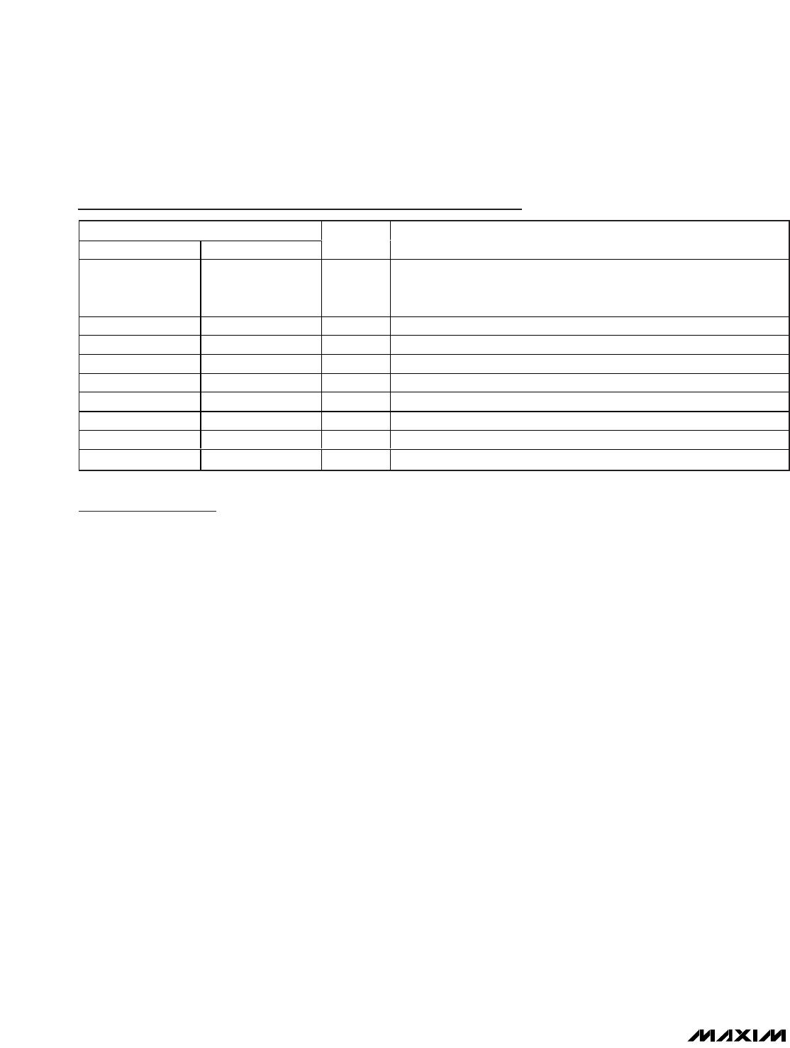
Pin Description (continued)
PIN
SSOP/TSSOP TQFN-EP
NAME FUNCTION
911V
DDF
Positive Supply Voltage for EEPROM. Connect a 1µF capacitor from
V
DDF
to V
SS
. Connect V
DDF
to V
DD
or for improved noise performance
connect a 30Ω resistor to V
DD
.
10 12 UNLOCK Secure-Lock Disable. Allows communication to the device.
11 14 DIO Digital Input Output. DIO allows communication with the device.
12 15 CLK1M 1MHz Clock Output. The output can be controlled by a configuration bit.
13 17 AMPOUT Uncommitted Amplifier Output
14 18 AMP- Uncommitted Amplifier Negative Input
15 19 AMP+ Uncommitted Amplifier Positive Input
16 21 FSOTC Full Span TC Buffered Output
EP Exposed Pad (TQFN Only). Internally connected; connect to V
SS
.

MAX1452ATG+T

Mfr. #:
Manufacturer:
Maxim Integrated
Description:
Sensor Interface LO-COST PREC SNSR SIGNAL CDTNR
Lifecycle:
New from this manufacturer.
Delivery:
DHL FedEx Ups TNT EMS
Payment:
T/T Paypal Visa MoneyGram Western Union