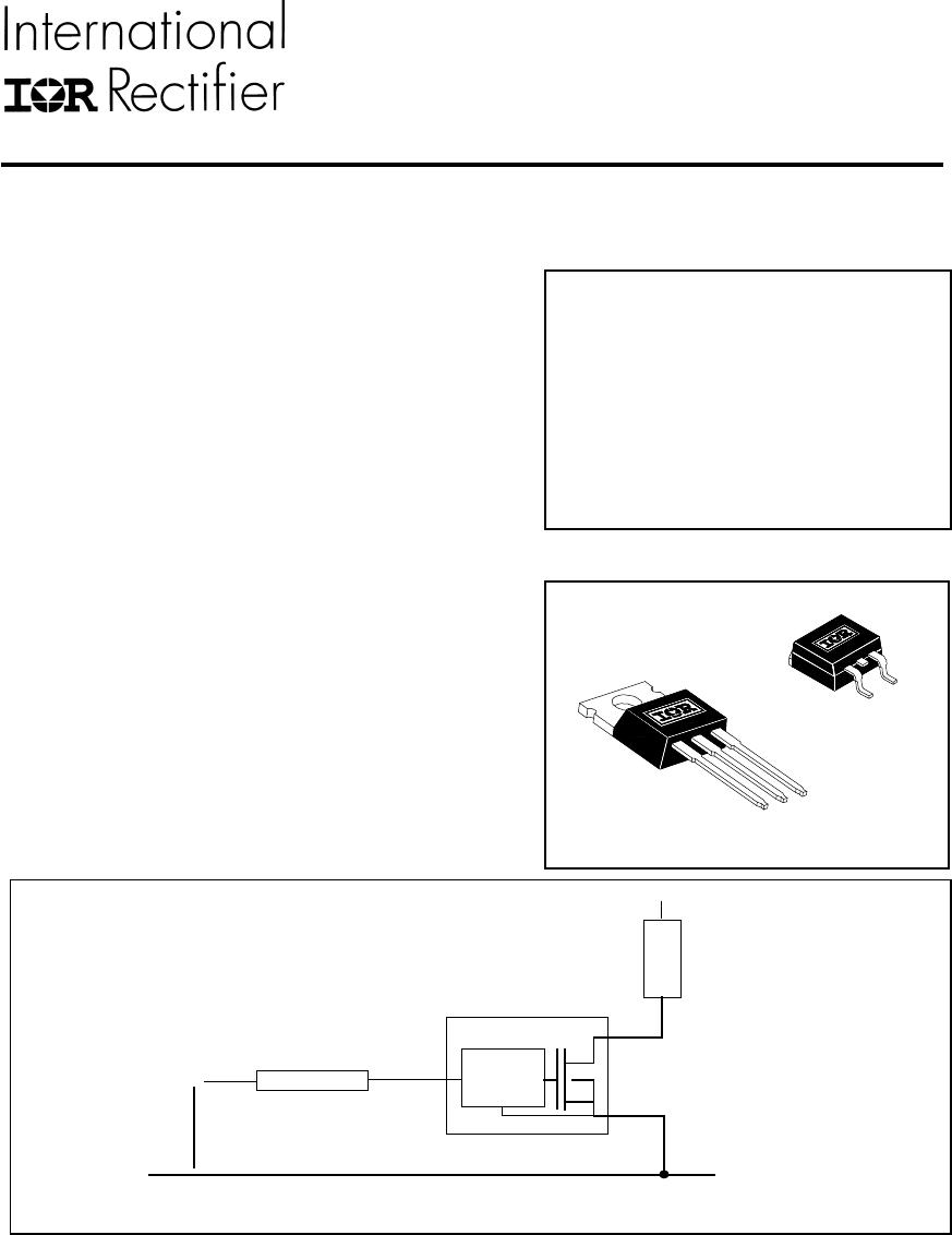
IPS021(S)
2 www.irf.com
(1) Limited by junction temperature (pulsed current limited also by internal wiring)
(2) Operations at higher switching frequencies is possible. See Appl. Notes.
Absolute Maximum Ratings
Absolute maximum ratings indicate sustained limits beyond which damage to the device may occur. All voltage parameters
are referenced to SOURCE lead. (T
Ambient
= 25
o
C unless otherwise specified). PCB mounting uses the standard foot-
print with 70 µm copper thickness.
Symbol Parameter Min. Max. Units Test Conditions
V
ds
Maximum drain to source voltage — 47
V
in
Maximum input voltage -0.3 7
I
in, max
Maximum IN current -10 +10 mA
I
sd cont.
Diode max. continous current
(1)
(rth=62
o
C/W) IPS021 — 2.8
(rth=10
o
C/W) IPS021 — 8
(rth=80
o
C/W) IPS021S — 2.2
I
sd pulsed
Diode max. pulsed current
(1)
— 10A
P
d Maximum power dissipation
(1)
(rth=62
o
C/W) IPS021 — 2
(rth=80
o
C/W) IPS021S — 1.56
ESD1 Electrostatic discharge voltage (Human Body) — 4 C=100pF, R=1500Ω,
ESD2 Electrostatic discharge voltage (Machine Model) — 0.5 C=200pF, R=0Ω, L=10µH
T
stor.
Max. storage temperature -55
150
T
j
max. Max. junction temperature. -40
150
T
lead
Lead temperature (soldering, 10 seconds) — 300
V
W
A
kV
o
C
Symbol Parameter Min. Typ. Max. Units Test Conditions
R
th
1 Thermal resistance free air — 60 —
R
th
2 Thermal resistance junction to case — 5
—
R
th
1 Thermal resistance with standard footprint — 80 —
R
th
2 Thermal resistance with 1" square footprint — 50 —
R
th
3 Thermal resistance junction to case — 5 —
Thermal Characteristics
TO-220
D
2
PAK (SMD220)
o
C/W
Recommended Operating Conditions
These values are given for a quick design. For operation outside these conditions, please consult the application notes.
Symbol Parameter Min. Max. Units
V
ds
(max) Continuous drain to source voltage
—
35
V
IH
High level input voltage 4 6
V
IL
Low level input voltage
0 0.5
I
ds
Continuous drain current — 1.8 A
Tamb=85
o
C (
TAmbient = 85
o
C, IN = 5V, rth = 60
o
C/W, Tj = 125
o
C)
R
in
Recommended resistor in series with IN pin 0.5
5 k
Ω
T
r-in (max)
Max recommended rise time for IN signal (see fig. 2) — 1
µ
S
F
r
-I
sc
(2)
Max. frequency in short circuit condition (Vcc = 14V) 0 1 kHz
V