Expand menu
Hello, Sign in
My Account
0
Cart
Home
Products
Sensors
Semiconductors
Passive Components
Connectors
Power
Electromechanical
Optoelectronics
Circuit Protection
Integrated Circuits - ICs
Main Products
Manufacturers
Blog
Services
About OMO
About Us
Contact Us
Check Stock
IPS021S
P1-P3
P4-P6
P7-P9
P10-P12
IPS021(S)
4
www
.irf
.com
Lead Assignments
Part Number
1 2 3
In D
S
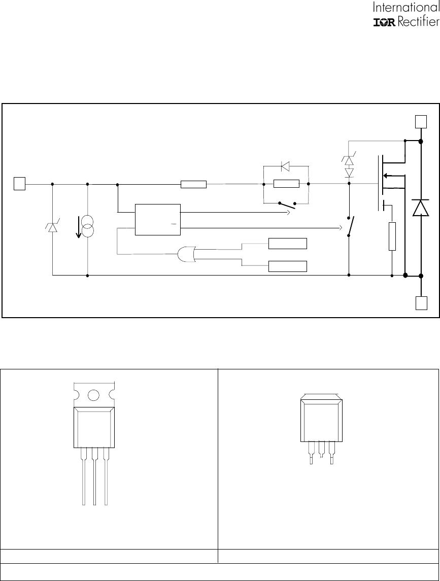
TO-220
IPS021
2 (D)
D
2
PAK (SMD220)
IPS021S
1 3
I
n
D
S
2 (D)
Functional Block Diagram
All values are typical
IN
DRAI
N
SOURCE
8.1 V
80
µ
A
47 V
I sen
se
200 k
Ω
1000
Ω
S
Q
R
Q
T > 165°c
I > Isd
IPS021(S)
www
.irf
.com
5
14 V
IN
D
S
5 v
0 v
L
R
+
-
Vds
Id
s
Vin
V load
Rem :
V
lo
ad is
neg
ativ
e
d
ur
ing
d
emag
ne
t
izat
io
n
Figure 4 - Active clamp test circuit
Id
s
Vds
Vin
T clam
p
Vd
s cl
am
p
(
Vcc
)
( s
ee App
l . Note
s to
eval
uate po
wer di
ssip
ation
)
Figure 3 - Active clamp waveforms
Figure 1 - Timing diagram
Tr
-in
10 %
90 %
90 %
10 %
Td
on
Td
off
tf
tr
Id
s
Tr
-in
V
i
n
Vds
Figure 2 - IN rise time & switching time definitions
T
s
d
(165
°
c)
Vin
Ids
Isd
I sh
ut
down
T
T shutdown
t < T r
ese
t
t > T r
ese
t
5 V
0 V
IPS021(S)
6
www
.irf
.com
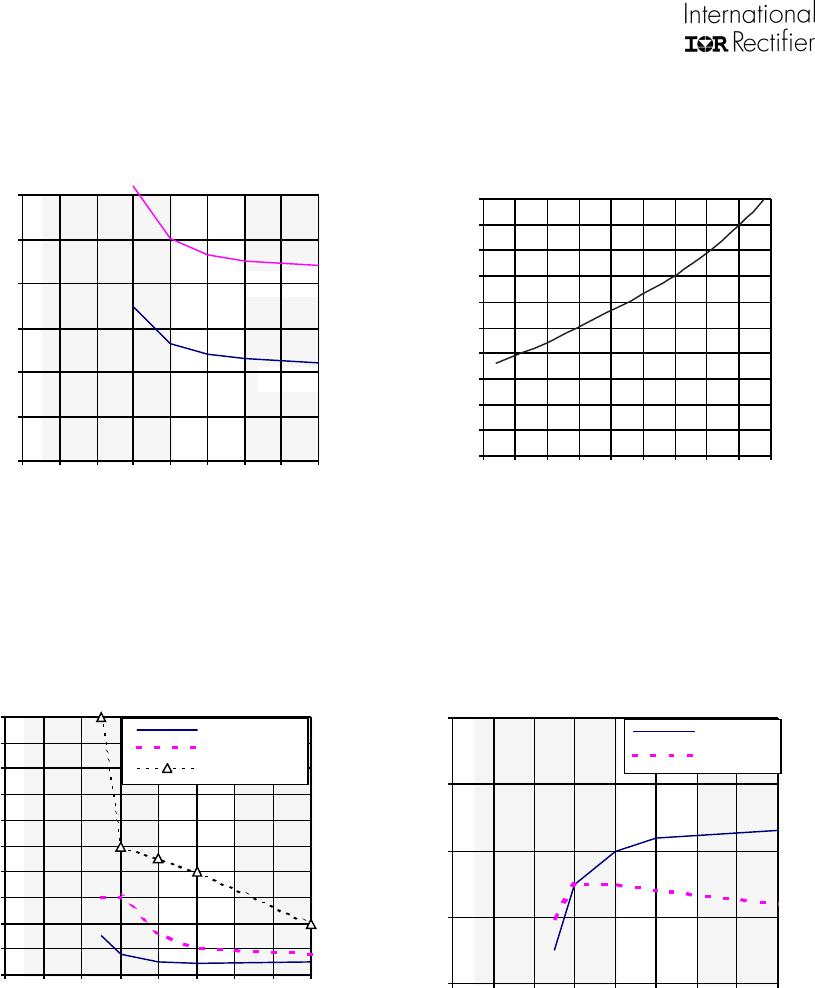
All curves are typical values with standard footprints. Operating in the shaded area is not recommended.
Figure 6 - Normalized Rds(on) (%) Vs Tj (
o
C)
Figure 5 - Rds ON (m
Ω
) Vs Input Voltage (V)
Tj = 150
o
C
Tj = 25
o
C
0
50
100
150
200
250
300
012
3456
78
0%
20%
40%
60%
80%
100%
120%
140%
160%
180%
200%
-
50
-
25
0
25
50
75
100
125
150
175
Figure 8 - Turn-OFF Delay Time & Fall Time (us)
Vs Input Voltage (V)
Figure 7 - Turn-ON Delay Time, Rise Time & Time
to 130% final Rds
(on)
(us) Vs Input Voltage (V)
0
1
2
3
4
5
6
7
8
9
10
01
23
45
67
8
ton d
e
la
y
ri
se ti
m
e
130%
r
d
s
o
n
0
1
2
3
4
012
34
56
78
tof
f de
l
a
y
fa
l
l ti
m
e
P1-P3
P4-P6
P7-P9
P10-P12
IPS021S
Mfr. #:
Buy IPS021S
Manufacturer:
Infineon Technologies
Description:
Gate Drivers IR_HSS-LSS-GATEDRIVER
Lifecycle:
New from this manufacturer.
Delivery:
DHL
FedEx
Ups
TNT
EMS
Payment:
T/T
Paypal
Visa
MoneyGram
Western
Union
Products related to this Datasheet
IPS021S
IPS021STRL
IPS021