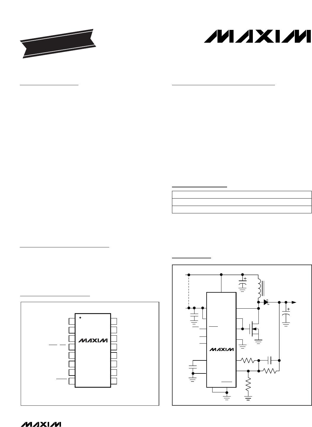
General Description
The MAX1620/MAX1621 convert a 1.8V to 20V battery
voltage to a positive or negative LCD backplane bias
voltage. Backplane bias voltage can be automatically
disabled when the display logic voltage is removed,
protecting the display. These devices use very little PC
board area, come in ultra-small QSOP packages, and
require only small, low-profile external components.
Output voltage can be set to a desired positive or nega-
tive voltage range with external resistors, and adjusted
over that range with the on-board digital-to-analog con-
verter (DAC) or with a potentiometer. The MAX1620/
MAX1621 include a 5-bit DAC, allowing digital software
control of the bias voltage. The MAX1620 uses up/down
digital signaling to adjust the DAC, and the MAX1621
uses the System Management Bus (SMBus™) 2-wire
serial interface.
These devices use a low-cost, external, N-channel MOSFET
power switch or NPN transistor, and can be configured
for positive or negative output voltages. Operating cur-
rent is a low 150µA, typically provided from a display’s
logic supply of 3.0V to 5.5V. The MAX1620/MAX1621 are
available in a 16-pin QSOP package.
Applications
Notebook Computers
Palmtop Computers
Personal Digital Assistants
Portable Data-Collection Terminals
Features
1.8V to 20V Battery Input Voltage
Automatic Disable when Display Logic
is Shut Down
Extremely Small QSOP Package
32-Level Internal DAC
SMBus Serial Interface (MAX1621)
Positive or Negative Output Voltage
MAX1620/MAX1621
Digitally Adjustable LCD Bias Supplies
________________________________________________________________
Maxim Integrated Products
1
PART
MAX1620EEE
MAX1621EEE
-40°C to +85°C
-40°C to +85°C
TEMP. RANGE PIN-PACKAGE
16 QSOP
16 QSOP
EVALUATION KIT MANUAL
FOLLOWS DATA SHEET
Ordering Information
19-1214; Rev 1; 1/98
LX
DHI
DLO
PGND
DOUT
FB
V
DD
POL
SHDN
DN
UP
REF
AGND
MAX1620
12.5V
TO
23.5V OUT
2V TO
12V
3V TO
5.5V
ON
/
OFF
DOWN
UP
LCDONPOK
BATT
Typical Operating Circuit
SMBus is a trademark of Intel Corp.
Pin Configuration
16
15
14
13
12
11
10
9
1
2
3
4
5
6
7
DHI
DLO
LX
PGND
AGND
V
DD
DOUT
FB
DN (SDA)
UP (SCL)
BATT
SHDN (SUS)
POK
REF
POL
LCDON
TOP VIEW
MAX1620
MAX1621
QSOP
( ) ARE FOR MAX1621 ONLY.
8
For free samples & the latest literature: http://www.maxim-ic.com, or phone 1-800-998-8800.
For small orders, phone 1-800-835-8769.
MAX1620/MAX1621
Digitally Adjustable LCD Bias Supplies
2 _______________________________________________________________________________________
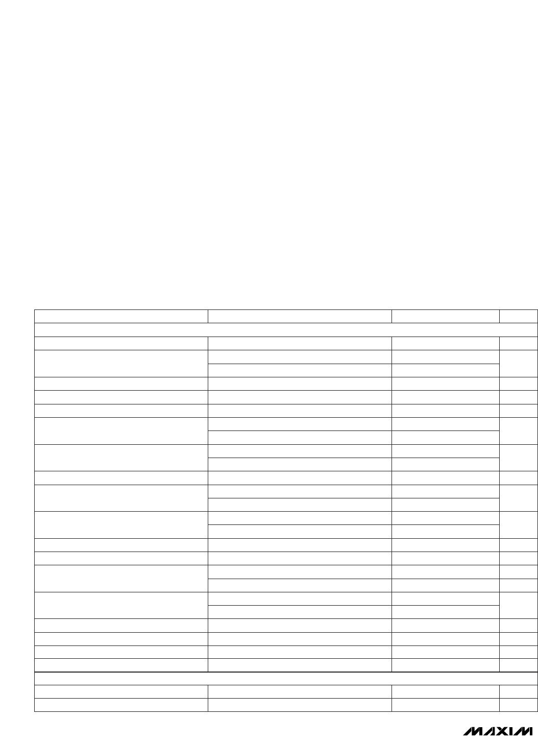
ABSOLUTE MAXIMUM RATINGS
ELECTRICAL CHARACTERISTICS
(V
DD
= 3.3V, V
BATT
= 10V, T
A
= 0°C to +85°C, unless otherwise noted.)
Stresses beyond those listed under “Absolute Maximum Ratings” may cause permanent damage to the device. These are stress ratings only, and functional
operation of the device at these or any other conditions beyond those indicated in the operational sections of the specifications is not implied. Exposure to
absolute maximum rating conditions for extended periods may affect device reliability.
V
DD
to AGND..............................................................-0.3V to 6V
PGND to AGND ..................................................................±0.3V
BATT, LX,
LCDON to AGND....................................-0.3V to 30V
DHI, DLO to PGND.....................................-0.3V to (V
DD
+ 0.3V)
DOUT, FB, POL, POK, REF to AGND.........-0.3V to (V
DD
+ 0.3V)
UP, DN, SHDN to AGND.............................................-0.3V to 6V
SCL, SDA, SUS to AGND............................................-0.3V to 6V
I
DHI
......................................................................................60mA
I
DLO
....................................................................................-30mA
I
LCDON
...............................................................................-10mA
Continuous Power Dissipation (T
A
= +70°C)
QSOP (derate 8.3mW/°C above +70°C) ......................667mW
Operating Temperature Range
MAX1620EEE/MAX1621EEE ............................-40°C to +85°C
Storage Temperature Range.............................-65°C to +150°C
Lead Temperature (soldering, 10sec).............................+300°C
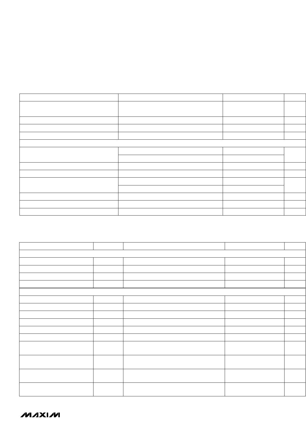
V
LCDON
= 28V, POK = 0.967V
V
LCDON
= 0.4V, POK = 1.017V
FB = -50mV
FB = REF + 100mV
POL = AGND, 3.0V V
DD
5.5V
Shutdown mode, V
SHDN
= V
DD
,V
DD
= 5.5V
POL = V
DD
, 3.0V V
DD
5.5V
Operating mode, output in regulation, V
DD
= 5.5V
V
DD
= 5V
V
DD
= 5V
V
DD
= 3.0V
LX = 12V, shutdown mode
V
DD
= 4.5V
LX = 12V, operating mode
BATT = 12V, shutdown mode
4V BATT 12V, T
A
= 0°C to +85°C
BATT = 12V, operating mode
1.8V BATT 20V, T
A
= +25°C
µA1
LCDON High, Leakage Current
mA-2 -6
LCDON Low, Sinking Current
nA
-10 85
-20 10
FB Input Current (Note 3)
mV-8 0 8
V1.46 1.5 1.53
FB Regulation Voltage
mA-25DLO Output Current (Note 3)
mA50DHI Output Current (Note 3)
14
7
On-Resistance (DLO, DHI)
16.5 23.5
µs-V
20
Microsecond-Volt Time Constant (k-factor)
V27Positive Output Voltage
920
µA
150 250
V
DD
Supply Current
1.8 20BATT Operating Range (Note 2)
1
µA
13 20
LX Input Current
µA
1
BATT Input Current
-27Negative Output Voltage
V1.5 2.8Undervoltage Lockout Threshold (Note 1)
13 20
V3.0 5.5V
DD
Operating Range
Voltage on POK rising V0.967 0.992 1.017POK Threshold Voltage
V
mV12POK Hysteresis
CONDITIONS UNITS
MIN TYP MAX
PARAMETER
V
No load V1.47 1.5 1.53REF Voltage
0µA I
REF
25mA mV310REF Load Regulation
SWITCHING REGULATOR
REFERENCE AND DAC OUTPUT
MAX1620/MAX1621
Digitally Adjustable LCD Bias Supplies
_______________________________________________________________________________________
3
ELECTRICAL CHARACTERISTICS (continued)
(V
DD
= 3.3V, V
BATT
= 10V, T
A
= 0°C to +85°C, unless otherwise noted.)
TIMING CHARACTERISTICS
(T
A
= 0°C to +85°C, unless otherwise noted.)
-20µA I
DOUT
0µA
I
SDA
= -6mA
V
IN
= 0V or V
IN
= V
DD
V
DD
= 5.5V
V
DD
= 5.5V
3.0V V
DD
3.6V
3.0V V
DD
3.6V
48.39mV step size
V
IN
= 0V or V
IN
= V
DD
Guaranteed monotonic
0µA I
DOUT
40µA
V0.4
µA±1
SCL, SDA, SUS Input Leakage Current
V0.6
SCL, SDA, SUS Input Low Voltage
V
2.3
1.4
SCL, SDA, SUS Input High Voltage
±1
V
0.6
V0 0.007DOUT Minimum Output Voltage (Note 3)
2.3
V
1.4
UP, DN, SHDN, POL Input High Voltage
LSBDOUT Differential Nonlinearity
Bits5DOUT Resolution
±1
REF - REF +
0.02 0.02
DOUT Maximum Output Voltage (Note 3) V
UP, DN, SHDN, POL Input Leakage Current
µA
UP, DN, SHDN, POL Input Low Voltage
SDA Output Low Voltage
CONDITIONS UNITSMIN TYP MAXPARAMETER
DIGITAL INPUTS AND OUTPUTS
(Note 4)
(Note 4)
(Note 4)
CONDITIONS
1
SCL Falling Edge to SDA Valid
Master Clocking in Data
µst
DV
µs4t
HD:STA
Start Condition SDA to SCL
Hold Time
µs4.7t
SU:STA
Start Condition SCL to SDA
Setup Time
µs4t
HIGH
SCL High Time
µs4.7t
LOW
SCL Low Time
ns300t
F
SCL/SDA Fall Time
µs1t
1
Pulse Width High (UP, DN)
µs1t
R
SCL/SDA Rise Time
ns0t
HD:DAT
SCL to SDA Data-Hold Time
ns500t
SU
:
DAT
SDA to SCL Data-Setup Time
µs1t
2
Pulse Width Low (UP, DN)
µs1t
3
Pulse Separation (UP, DN)
µs1t
4
Counter Reset Time
UNITSMIN TYP MAXSYMBOLPARAMETER
µs4t
SU:STO
Stop Condition SCL_ to SDA_
Setup Time
MAX1620 (Figure 1)
MAX1621 (Figures 2 and 3)

MAX1620EEE+

Mfr. #:
Manufacturer:
Maxim Integrated
Description:
Power Management Specialized - PMIC Digitally Adjustable LCD Bias Supply
Lifecycle:
New from this manufacturer.
Delivery:
DHL FedEx Ups TNT EMS
Payment:
T/T Paypal Visa MoneyGram Western Union

Products related to this Datasheet