MAX1620/MAX1621
Digitally Adjustable LCD Bias Supplies
10 ______________________________________________________________________________________
R1
360k
2V
TO
12V
BATT
POK
D1
MBRS0540
N1
MMFT3055VL
Q1
MMBT2907
V
DD
POL
SHDN (SUS)
DN (SDA)
UP (SCL)
REF
AGND
3
5
OPTIONAL
11
7
4
1
2
6
12
( ) ARE FOR MAX1621.
NOTE: CONNECTIONS TO DIGITAL INPUTS NOT SHOWN.
14
16
15
13
R3
300k
R4
300k
R5
2.2M
C6
100pF
10
9
8
LX
DHI
DLO
PGND
DOUT
FB
LCDON
3V
TO
5.5V
C1
0.1µF
C2
0.1µF
R2
100k
R8
10k
TO REF
D3 1N6263 (ANY SCHOTTKY)
C3
22µF
C5
22µF
12.5V
TO
23.5V OUT
VOUTSW
OPTIONAL
R6
56k
R7
56k
L1
100µH
MAX1620
MAX1621
U1
_______________Detailed Description
The MAX1620/MAX1621 are step-up power controllers
that drive an external N-channel FET or NPN transistor
to convert power from a 1.8V to 20V battery to a higher
positive or negative voltage. They are configured as
negative-output, inverting power controllers with one
additional diode and one additional capacitor. Either
configuration’s output voltage can be adjusted with
external resistors, or digitally adjusted with an internal
digital-to-analog converter (DAC). The MAX1620 uses
pin-defined controls for the DAC, while the MAX1621
communicates with the DAC via the SMBus™ interface.
Operating Principle
The MAX1620/MAX1621 operate in discontinuous-
conduction mode (where the inductor current ramps to
zero by the end of each switching cycle) and with a
constant peak current, without requiring a current-
sense resistor. Switch on-time is inversely proportional
to the input voltage V
BATT
by a microsecond-volt con-
stant, or k-factor, of 20µs-V (e.g., for V
BATT
= 10V,
on-time = 2µs).
For an ideal boost converter operating in discontinu-
ous-conduction mode (no power losses), output current
is proportional to input voltage and peak inductor current:
I
PK
is proportional to on-time (t
ON
), which, for these
parts, is determined by the k-factor:
I
PK
= k-factor / L
Discontinuous conduction is detected by monitoring the
LX node voltage. When the inductor’s energy is com-
pletely delivered, the LX node voltage snaps back to
the BATT voltage. When this crossing is sensed, anoth-
er pulse is issued if the output is still out of regulation.
Positive Output Voltage
To select a positive output voltage, tie the polarity pin
(POL) to V
DD
and use the typical boost topology shown
in Figure 4. FB regulation voltage is 1.5V. For optimum
stability, V
OUT
should be greater than 1.1 (V
BATT
).
Negative Output Voltage
To select a negative output voltage, tie POL to GND
(Figure 5). In this configuration, the internal error amplifi-
er’s output is inverted to provide the correct feedback
polarity. FB regulation voltage is 0V. D1, D2, C4, and C5
form an inverting charge pump to generate the negative
voltage. This allows application of the positive boost
switching topology to negative output voltages.
The negative output circuit has two possible connec-
tions. In the standard connection, D1’s cathode is con-
nected to BATT. This connection features the best
output ripple performance, but V
OUT
must be limited
to no more than 27V - 1.1(V
BATT
). If a larger negative
voltage is needed, an alternative connection allows a
maximum negative output of -27V, but with the addition-
al constraint that V
OUT
> 1.1V
BATT
. To use the alter-
native circuit, connect D1’s cathode to ground rather
than BATT (Figure 6). Increase C4 to 2.2µF to improve
output ripple performance.
The negative charge pump limits the output current to
the charge transferred each cycle multiplied by the
I
1
2
I V / V
OUT PK BATT OUT
×
Figure 4. Typical Operating Circuit—Positive Output
MAX1620/MAX1621
Digitally Adjustable LCD Bias Supplies
______________________________________________________________________________________ 11
maximum switching frequency. The following equation
represents the output current for the ideal case (no
power losses) of Figure 5:
This means that a higher peak current is required to
achieve the same output current in the negative output
circuit as in the positive output circuit.
The output current for Figure 6 uses the same current
equation as the positive boost.
Output Voltage Control
The output voltage is set with a voltage divider to the
feedback pin (FB). For a positive output, the divider is
referred to GND; for a negative output, the divider is
referred to REF.
Output voltage can be adjusted with an internal DAC
summing current into FB through an external resistor.
The 5-bit DAC is controlled with a user-programmable
up/down counter. On power-up or after a reset, the
counter sets the DAC output to 10000 binary, or half-
scale.
I x (k -factor / L) x V / (V V )
OUT BATT BATT OUT
=+
1
2
2V
TO
15V
BATT
POK
N1
MMFT3055VL
V
DD
POL
SHDN (SUS)
DN (SDA)
UP (SCL)
REF
AGND
3
5
11
7
4
1
2
6
12
( ) ARE FOR MAX1621.
NOTE: CONNECTIONS TO DIGITAL INPUTS NOT SHOWN.
14
16
15
13
R3
300k
R4
300k
R5
1.2M
C6
100pF
10
9
8
LX
DHI
DLO
PGND
DOUT
FB
LCDON
3V
TO
5.5V
C1
0.1µF
C2
0.1µF
C3
22µF
C5
22µF
-6V
TO
-12V OUT
L1
100µH
D1
MBRS0540
D2
MBRS0540
C4
1µF
MAX1620
MAX1621
U1
R8
10k
TO REF
D3 1N6263 (ANY SCHOTTKY)
2V
TO
12V
BATT
POK
N1
MMFT3055VL
V
DD
POL
SHDN (SUS)
DN (SDA)
UP (SCL)
REF
AGND
3
5
11
7
4
1
2
6
12
( ) ARE FOR MAX1621.
NOTE: CONNECTIONS TO DIGITAL INPUTS NOT SHOWN.
14
16
15
13
R3
300k
R4
300k
R5
2.7M
C6
100pF
10
9
8
LX
DHI
DLO
PGND
DOUT
FB
LCDON
3V
TO
5.5V
C1
0.1µF
C2
0.1µF
C3
22µF
C5
22µF
-13.5V
TO
-27V OUT
L1
100µH
D2
MBRS0540
D1
MBRS0540
C4
2.2µF
MAX1620
MAX1621
U1
R8
10k
TO REF
D3 1N6263 (ANY SCHOTTKY)
Figure 5. Typical Operating Circuit—Negative Output
Figure 6. Alternative Negative Output—Maximum Voltage
MAX1620/MAX1621
Digitally Adjustable LCD Bias Supplies
12 ______________________________________________________________________________________
The MAX1620 controls the DAC counter with the UP
and DN pins. A rising edge on UP increases V
OUT
by
decrementing the counter and decreasing the DAC
output voltage one step; a rising edge on DN de-
creases V
OUT
by incrementing the counter and
increasing the DAC output voltage one step. Holding
both UP and DN high resets the counter to half-scale.
The counter will not roll over at either the FS or ZERO
code. The control direction of UP and DN reverses for a
negative output, to maintain the same control direction
of the output voltage in absolute magnitude.
The MAX1621 controls the counter to the DAC through
the SMBus interface. The counter is treated as a 5-bit
register and resets on power-up. The setting in the DAC
is guaranteed to remain valid as long as V
DD
is greater
than the UVLO threshold (see Note 1 in the
Electrical
Characteristics
).
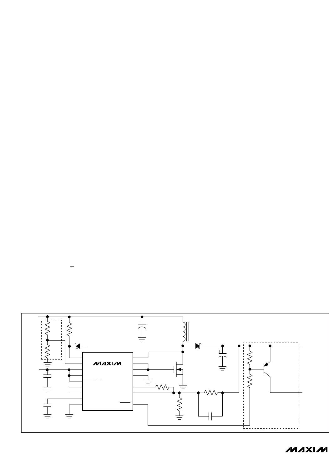
The MAX1620/MAX1621’s open-drain DMOSFET
(LCDON) can be used to disconnect the LCD panel
from the positive bias voltage with an external transistor.
The FET turns off (LCDON = float) if power-OK voltage
(POK) falls below 1V. In the MAX1621, LCDON can also
be controlled by the SMB command. LCDON cannot
switch negative output voltages.
To prevent uncontrolled boosting when the output is
disconnected, the feedback resistors must sense the
boosted voltage rather than the output of the LCDON
switch (Figure 4).
Shutdown Mode
The MAX1620 shuts down when the SHDN pin is low.
The internal reference and biasing circuitry turn off,
and the supply current drops to 9µA. In shutdown,
DOUT = 0V and LCDON floats. UP/DN are ignored to
preserve the DAC state for the MAX1620. Tie unused
logic inputs to AGND for lowest operating current.
The MAX1621 can be shut down using the SMBus
interface (Table 2).
Reset Modes
If the MAX1620 is not in shutdown mode, the DAC can
be reset to mid-scale by holding UP and DN high. Mid-
scale is 16 steps from the minimum DAC output and 15
steps from the maximum.
The MAX1620/MAX1621 reset the DAC counter to mid-
scale at power-up or when V
DD
is below the undervolt-
age lockout threshold of 2.2V (typ).
MAX1621 Digital Interface
A single byte of data written over the Intel SMBus con-
trols the MAX1621. Figures 7 and 8 show example
single-byte writes. The MAX1621 contains two 2-bit reg-
isters for storing configuration data, and one register for
the 5-bit DAC data. Tables 1 and 2 describe the data
format for the configuration registers. The MAX1621
responds only to its own address (0101100 binary).
The REGSEL bit addresses the configuration registers.
REGSEL = 0 for the SUS register; REGSEL = 1 for the
OPR register. Each configuration register consists of a
SHDN bit and an LCDON bit. One of the two configura-
tion registers is always active. The state of the SUS pin
determines the active register. The OPR register is active
with SUS = high. The SUS register is active with SUS =
low.
Each byte written to the MAX1621 updates the DAC reg-
ister. DAC data is preserved in shutdown and when tog-
gling between configuration registers. Since there is only
one DAC register, SUS cannot be used to toggle
between two DAC codes.
Status information can be read from the MAX1621 using
the SMBus read-byte protocol. Figure 9 shows an exam-
ple status read and Table 3 describes the status-
information format.
During shutdown (SUS = 1 and OPR-SHDN = 0, or
SUS = 0 and SUS-SHDN = 0), the MAX1621 serial inter-
face remains fully functional and can be used to set
either the OPR-SHDN or SUS-SHDN bits to return the
MAX1621 to its normal operational state.
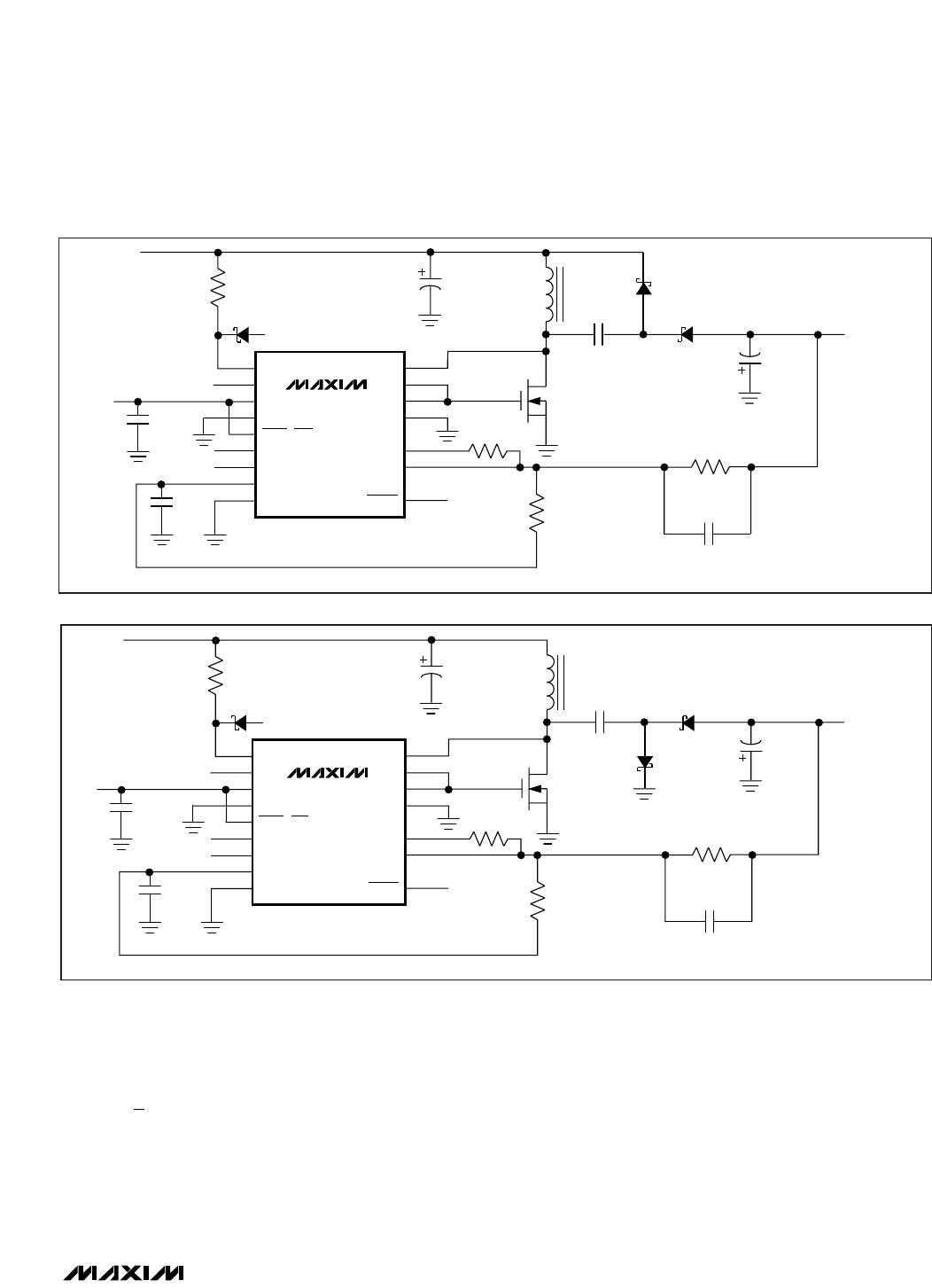
Separate/Same Power for L1 and V
DD
Separate voltage sources can supply the inductor (L1)
and the IC (V
DD
). This allows operation from low-voltage
batteries as well as high-voltage sources because chip
bias (150µA) is provided by a logic supply (3V to 5.5V)
while output power is sourced directly from the battery
to L1. Conversely, L1 and V
DD
can also be supplied
from one supply if it remains with V
DD
’s operating limits
(3V to 5.5V). If L1 and V
DD
are fed from the same volt-
age, D3 and R8 (Figures 4, 5, 6, and 10) can be omit-
ted, and BATT may be connected directly to V
DD
.

MAX1620EEE+

Mfr. #:
Manufacturer:
Maxim Integrated
Description:
Power Management Specialized - PMIC Digitally Adjustable LCD Bias Supply
Lifecycle:
New from this manufacturer.
Delivery:
DHL FedEx Ups TNT EMS
Payment:
T/T Paypal Visa MoneyGram Western Union

Products related to this Datasheet