ADC0808S125_ADC0808S250_3 © NXP B.V. 2009. All rights reserved.
Product data sheet Rev. 03 — 24 February 2009 8 of 23
NXP Semiconductors
ADC0808S125/250
Single 8-bit ADC, up to 125 MHz or 250 MHz
7.5 Full-scale input selection
The ADC0808S has an internal reference circuit which can be overruled by an external
reference voltage. This can be done with the full-scale reference voltage (V
ref(fs)
)
according to Table 9.
The ADC provides the required common-mode voltage on pin CMADC. In case of internal
regulation, the regulator output voltage on pin CMADC is 0.95 V.
The internal reference circuit is enabled by connecting pin FSIN to ground. The
common-mode output voltage V
O(cm)
on pin CMADC will then be 0.95 V, and the
maximum peak-to-peak input voltage V
i(p-p)(max)
will be 2.0 V; see Figure 7 and Figure 8.
The ADC full-scale input selection principle is shown in Figure 9.
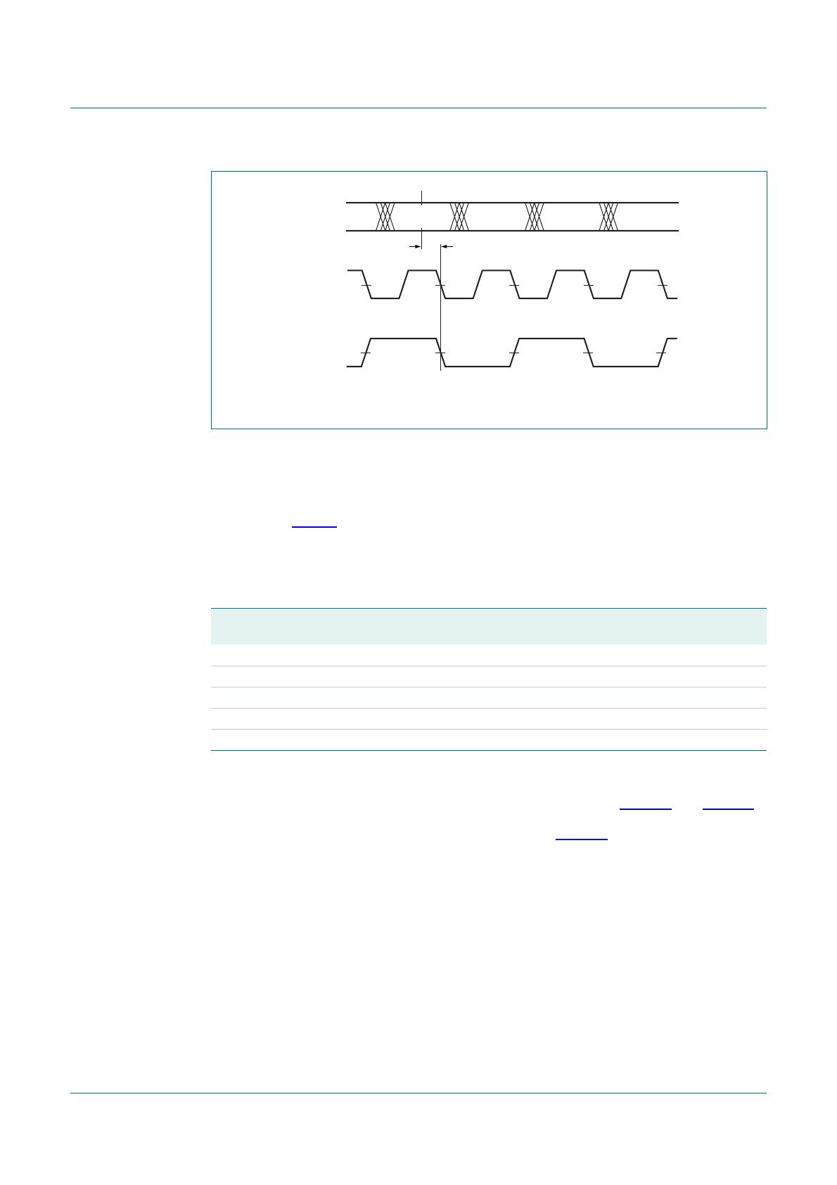
Fig 6. Complete conversion signal timing diagram using CCS
001aab893
CCS (f
clk
)
CCS (f
clk
/ 2)
D0 to D7
50 %
50 %
data
n − 2n − 1
data data data
n + 1n
t
d(CCS)
Table 9. Full-scale input selection
Full-scale reference voltage
V
ref(fs)
Common-mode output
voltage V
O(cm)
Maximum peak-to-peak input
voltage V
i(p-p)(max)
1.15 V 0.8 V 1.825 V
1.20 V 0.86 V 1.91 V
1.25 V 0.94 V 1.99 V
1.30 V 1.01 V 2.08 V
1.35 V 1.09 V 2.16 V