6
R
S
is perhaps the easiest to measure accurately. The V-I
curve is measured for the diode under forward bias, and
the slope of the curve is taken at some relatively high
value of current (such as 5 mA). This slope is converted
into a resistance R
d
.
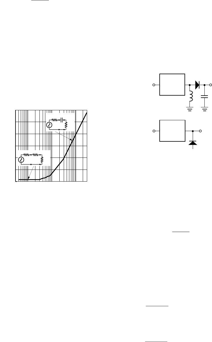
Detector Circuits
When DC bias is available, Schottky diode detec-
tor circuits can be used to create low cost RF and mi-
crowave receivers with a sensitivity of -55 dBm to
-57 dBm.
[1]
These circuits can take a variety of forms,
but in the most simple case they appear as shown in
Figure 8. This is the basic detector circuit used with the
HSMS-285x family of diodes.
In the design of such detector circuits, the starting point is
the equivalent circuit of the diode, as shown in Figure 6.
Of interest in the design of the video portion of the
circuit is the diode’s video impedance — the other
four elements of the equivalent circuit disappear at all
reasonable video frequencies. In general, the lower the
diode’s video impedance, the better the design.
[1]
Avago Application Note 923, Schottky Barrier Diode Video Detectors.
HSMS-285A/6A fig 10
INSERTION LOSS (dB)
3
-40
FREQUENCY (MHz)
-10
-25
3000
-20
10 1000100
-35
-30
-15
50 Ω
50 Ω
0.16 pF
50 Ω
50 Ω 9 KΩ
VIDEO
OUT
RF
IN
Z-MATCH
NETWORK
VIDEO
OUT
Z-MATCH
NETWORK
RF
IN
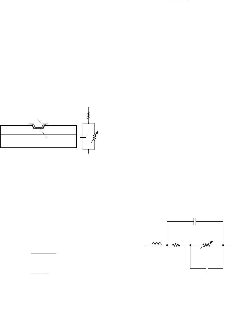
Figure 7. Measuring C
J
and R
V
.
At frequencies below 10 MHz, the video resistance dom-
inates the loss and can easily be calculated from it. At
frequencies above 300 MHz, the junction capacitance
sets the loss, which plots out as a straight line when
frequency is plotted on a log scale. Again, calculation is
straightforward.
L
P
and C
P
are best measured on the HP8753C, with the
diode terminating a 50 Ω line on the input port. The re-
sulting tabulation of S
11
can be put into a microwave
linear analysis program having the ve element equiv-
alent circuit with R
V
, C
J
and R
S
xed. The optimizer can
then adjust the values of L
P
and C
P
until the calculated
S
11
matches the measured values. Note that extreme
care must be taken to de-embed the parasitics of the
50 Ω test xture.
Figure 8. Basic Detector Circuits.
The situation is somewhat more complicated in the
design of the RF impedance matching network, which
includes the package inductance and capacitance
(which can be tuned out), the series resistance, the junc-
tion capacitance and the video resistance. Of these ve
elements of the diode’s equivalent circuit, the four para-
sitics are constants and the video resistance is a function
of the current owing through the diode.
R
V
and C
J
are very dicult to measure. Consider the
impedance of C
J
= 0.16 pF when measured at 1 MHz — it
is approximately 1 MΩ. For a well designed zero bias
Schottky, R
V
is in the range of 5 to 25 KΩ, and it shorts
out the junction capacitance. Moving up to a higher fre-
quency enables the measurement of the capacitance,
but it then shorts out the video resistance. The best mea-
surement technique is to mount the diode in series in a
50 Ω microstrip test circuit and measure its insertion loss
at low power levels (around -20 dBm) using an HP8753C
network analyzer. The resulting display will appear as
shown in Figure 7.
where
I
S
= diode saturation current in µA
I
b
= bias current in µA
Saturation current is a function of the diode’s design,
[2]
and
it is a constant at a given temperature. For the HSMS-285x
series, it is typically 3 to 5 µA at 25°C.
Saturation current sets the detection sensitivity, video re-
sistance and input RF impedance of the zero bias Schottky
detector diode. Since no external bias is used with the
HSMS-285x series, a single transfer curve at any given fre-
quency is obtained, as shown in Figure 2.
V - IR
S
I = I
S
(exp ( ) - 1)
0.026
0.026
I
f
26,000
R ≈
V
I
S
+ I
b
8.33 X 10
-5
n T
R
j
=
V
– R
s
I
S
+ I
b
0.026
= at 25°C
I
S
+ I
b
= R
R
S
= R
d
–
V - IR
S
I = I
S
(exp ( ) - 1)
0.026
0.026
I
f
26,000
R ≈
V
I
S
+ I
b
8.33 X 10
-5
n T
R
j
=
V
– R
s
I
S
+ I
b
0.026
= at 25°C
I
S
+ I
b
= R
R
S
= R
d
–