7
The most dicult part of the design of a detector circuit
is the input impedance matching network. For very
broadband detectors, a shunt 60 Ω resistor will give good
input match, but at the expense of detection sensitivity.
When maximum sensitivity is required over a narrow
band of frequencies, a reactive matching network
is optimum. Such networks can be realized in either
lumped or distributed elements, depending upon fre-
quency, size constraints and cost limitations, but certain
general design principals exist for all types.
[3]
Design
work begins with the RF impedance of the HSMS-285x
series, which is given in Figure 9.
[2]
Avago Application Note 969, An Optimum Zero Bias Schottky Detector Diode.
[3]
Avago Application Note 963, Impedance Matching Techniques for Mixers
and Detectors.
HSMS-285A/6A fig 13
1 GHz
2
3
4
5
6
0.2 0.6 1
2
5
HSMS-285A/6A fig 14
65nH
100 pF
VIDEO
OUT
RF
INPUT
WIDTH = 0.050"
LENGTH = 0.065"
WIDTH = 0.015"
LENGTH = 0.600"
TRANSMISSION LINE
DIMENSIONS ARE FOR
MICROSTRIP ON
0.032" THICK FR-4.
HSMS-285A/6A fig 15
FREQUENCY (GHz): 0.9-0.93
HSMS-285A/6A fig 16
RETURN LOSS (dB)
0.9
-20
FREQUENCY (GHz)
0.915
0
-10
-15
0.93
-5
Figure 9. RF Impedan
ce of the HSM
S-285x Series at-40 dBm.
915 MHz Detector Circuit
Figure 10 illustrates a simple impedance matching
network for a 915 MHz detector.
Figure 10. 915 MHz Matching Network for the HSMS-285x Series at Zero Bias.
A 65 nH inductor rotates the impedance of the diode to
a point on the Smith Chart where a shunt inductor can
pull it up to the center. The short length of 0.065" wide
microstrip line is used to mount the lead of the diodes
SOT-323 package. A shorted shunt stub of length <λ/4
provides the necessary shunt inductance and simul-
taneously provides the return circuit for the current
generated in the diode. The impedance of this circuit is
given in Figure 11.
Figure 11. Input Impedance.
The input match, expressed in terms of return loss, is
given in Figure 12.
Figure 12. Input Return Loss.
As can be seen, the band over which a good match is
achieved is more than adequate for 915 MHz RFID ap-
plications.
Voltage Doublers
To this point, we have restricted our discussion to single
diode detectors. A glance at Figure 8, however, will lead
to the suggestion that the two types of single diode de-
tectors be combined into a two diode voltage doubler
[4]
(known also as a full wave rectier). Such a detector is
shown in Figure 13.
Figure 13. Voltage Doubler Circuit.
8
Such a circuit oers several advantages. First the voltage
outputs of two diodes are added in series, increasing the
overall value of voltage sensitivity for the network (com-
pared to a single diode detector). Second, the RF imped-
ances of the two diodes are added in parallel, making
the job of reactive matching a bit easier. Such a circuit
can easily be realized using the two series diodes in the
HSMS-285C.
Flicker Noise
Reference to Figure 5 will show that there is a junc-
tion of metal, silicon, and passivation around the rim
of the Schottky contact. It is in this three-way junction
that icker noise
[5]
is generated. This noise can severely
reduce the sensitivity of a crystal video receiver utiliz-
ing a Schottky detector circuit if the video frequency is
below the noise corner. Flicker noise can be substantially
reduced by the elimination of passivation, but such
diodes cannot be mounted in non-hermetic packages.
p-type silicon Schottky diodes have the least icker noise
at a given value of external bias (compared to n-type
silicon or GaAs). At zero bias, such diodes can have
extremely low values of icker noise. For the HSMS-285x
series, the noise temperature ratio is given in Figure 14.
Any Schottky junction, be it an RF diode or the gate of
a MESFET, is relatively delicate and can be burned out
with excessive RF power. Many crystal video receivers
used in RFID (tag) applications nd themselves in poorly
controlled environments where high power sources may
be present. Examples are the areas around airport and
FAA radars, nearby ham radio operators, the vicinity of
a broadcast band transmitter, etc. In such environments,
the Schottky diodes of the receiver can be protected
by a device known as a limiter diode.
[6]
Formerly avail-
able only in radar warning receivers and other high cost
electronic warfare applications, these diodes have been
adapted to commercial and consumer circuits.
Avago oers a complete line of surface mountable
PIN limiter diodes. Most notably, our HSMP-4820 (SOT-
23) can act as a very fast (nanosecond) power-sensi-
tive switch when placed between the antenna and the
Schottky diode, shorting out the RF circuit temporar-
ily and reecting the excessive RF energy back out the
antenna.
Assembly Instructions
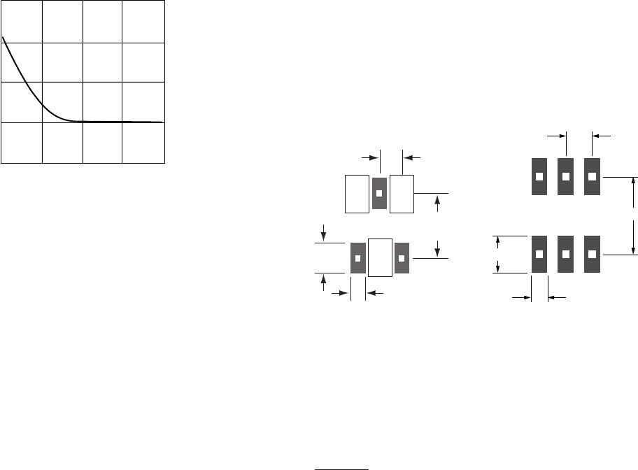
SOT-323 PCB Footprint
A recommended PCB pad layout for the miniature SOT-
323 (SC-70) package is shown in Figure 15 (dimensions
are in inches). This layout provides ample allowance for
package placement by automated assembly equipment
without adding parasitics that could impair the perfor-
mance. Figure 16 shows the pad layout for the six-lead
SOT-363.
[4]
Avago Application Note 956-4, Schottky Diode Voltage Doubler.
[5]
Avago Application Note 965-3, Flicker Noise in Schottky Diodes.
[6]
Avago Application Note 1050, Low Cost, Surface Mount Power Limiters.
NOISE TEMPERATURE RATIO (dB)
FREQUENCY (Hz)
15
10
5
0
-5
10 100 1000 10000 100000
Diode Burnout
Figure 14. Typical Noise Temperature Ratio.
Noise temperature ratio is the quotient of the diode’s
noise power (expressed in dBV/Hz) divided by the noise
power of an ideal resistor of resistance R = R
V
.
For an ideal resistor R, at 300°K, the noise voltage can be
computed from
v = 1.287 X 10
-10
R volts/Hz
which can be expressed as
20 log
10
v dBV/Hz
Thus, for a diode with R
V
= 9 KΩ, the noise voltage is
12.2 nV/Hz or -158 dBV/Hz. On the graph of Figure 14, -
158 dBV/Hz would replace the zero on the vertical scale
to convert the chart to one of absolute noise voltage vs.
frequency.
0.026
0.039
0.079
0.022
Dimensions in inches
0.026
0.075
0.016
0.035
Figure 15. Recommended PCB
Pad Layout for Avago’s SC70
3L/SOT-323 Products.
Figure 16. Recommended PCB Pad
Layout for Avago's SC70 6L/SOT-363
Products.
9
Figure 17. Surface Mount Assembly Prole.
SMT Assembly
Reliable assembly of surface mount components is a
complex process that involves many material, process,
and equipment factors, including: method of heating
(e.g., IR or vapor phase reow, wave soldering, etc.)
circuit board material, conductor thickness and pattern,
type of solder alloy, and the thermal conductivity and
thermal mass of components. Components with a low
mass, such as the SOT packages, will reach solder reow
temperatures faster than those with a greater mass.
Avagos diodes have been qualied to the time-tem-
perature prole shown in Figure 17. This prole is repre-
sentative of an IR reow type of surface mount assembly
process.
After ramping up from room temperature, the circuit
board with components attached to it (held in place
with solder paste) passes through one or more preheat
Lead-Free Reow Prole Recommendation (IPC/JEDEC J-STD-020C)
Reow Parameter Lead-Free Assembly
Average ramp-up rate (Liquidus Temperature (T
S(max)
to Peak) 3°C/ second max
Preheat Temperature Min (T
S(min)
) 150°C
Temperature Max (T
S(max)
) 200°C
Time (min to max) (t
S
) 60-180 seconds
Ts(max) to TL Ramp-up Rate 3°C/second max
Time maintained above: Temperature (T
L
) 217°C
Time (t
L
) 60-150 seconds
Peak Temperature (T
P
) 260 +0/-5°C
Time within 5 °C of actual
Peak temperature (t
P
)
20-40 seconds
Ramp-down Rate 6°C/second max
Time 25 °C to Peak Temperature 8 minutes max
Note 1: All temperatures refer to topside of the package, measured on the package body surface
25
Time
Temperature
Tp
T
L
tp
t
L
t 25° C to P eak
Ra mp-up
ts
Ts
min
Ramp-down
Preheat
Critical Zone
T
L
to Tp
Ts
max
zones. The preheat zones increase the temperature of
the board and components to prevent thermal shock
and begin evaporating solvents from the solder paste.
The reow zone briey elevates the temperature su-
ciently to produce a reow of the solder.
The rates of change of temperature for the ramp-up and
cool-down zones are chosen to be low enough to not
cause deformation of the board or damage to compo-
nents due to thermal shock. The maximum temperature
in the reow zone (T
MAX
) should not exceed 260°C.
These parameters are typical for a surface mount assem-
bly process for Avago diodes. As a general guideline, the
circuit board and components should be exposed only to
the minimum temperatures and times necessary to achieve
a uniform reow of solder.

HSMS-285C-BLKG

Mfr. #:
Manufacturer:
Broadcom / Avago
Description:
RF Detector RF/ID below 1.5GHz
Lifecycle:
New from this manufacturer.
Delivery:
DHL FedEx Ups TNT EMS
Payment:
T/T Paypal Visa MoneyGram Western Union