Low Skew, 1-to-9, Differential-to-
3.3V LVPECL Fanout Buffer
8531-01
Data Sheet
©2016 Integrated Device Technology, Inc Revision F January 19, 20161
GENERAL DESCRIPTION
The 8531-01 is a low skew, high performance
1-to-9 Differential-to-3.3V LVPECL Fanout
Buffer and a member of the family of High
Performance Clock Solutions from IDT. The
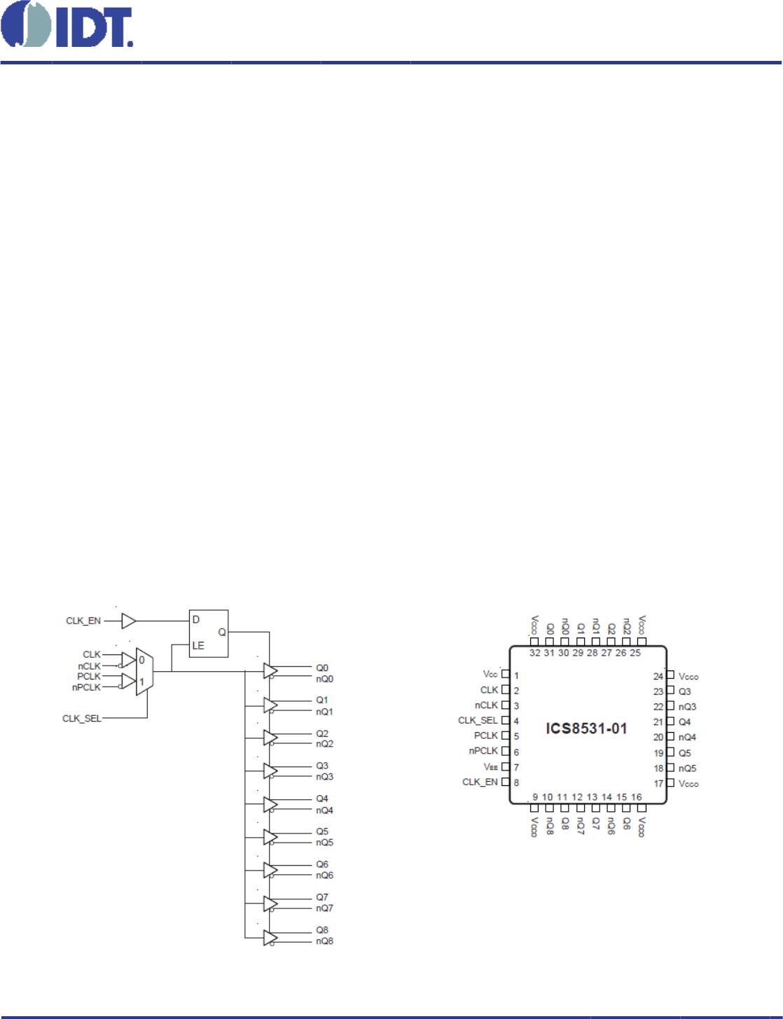
8531-01 has two selectable clock inputs. The CLK,
nCLK pair can accept most standard differential input
levels. The PCLK, nPCLK pair can accept LVPECL, CML, or
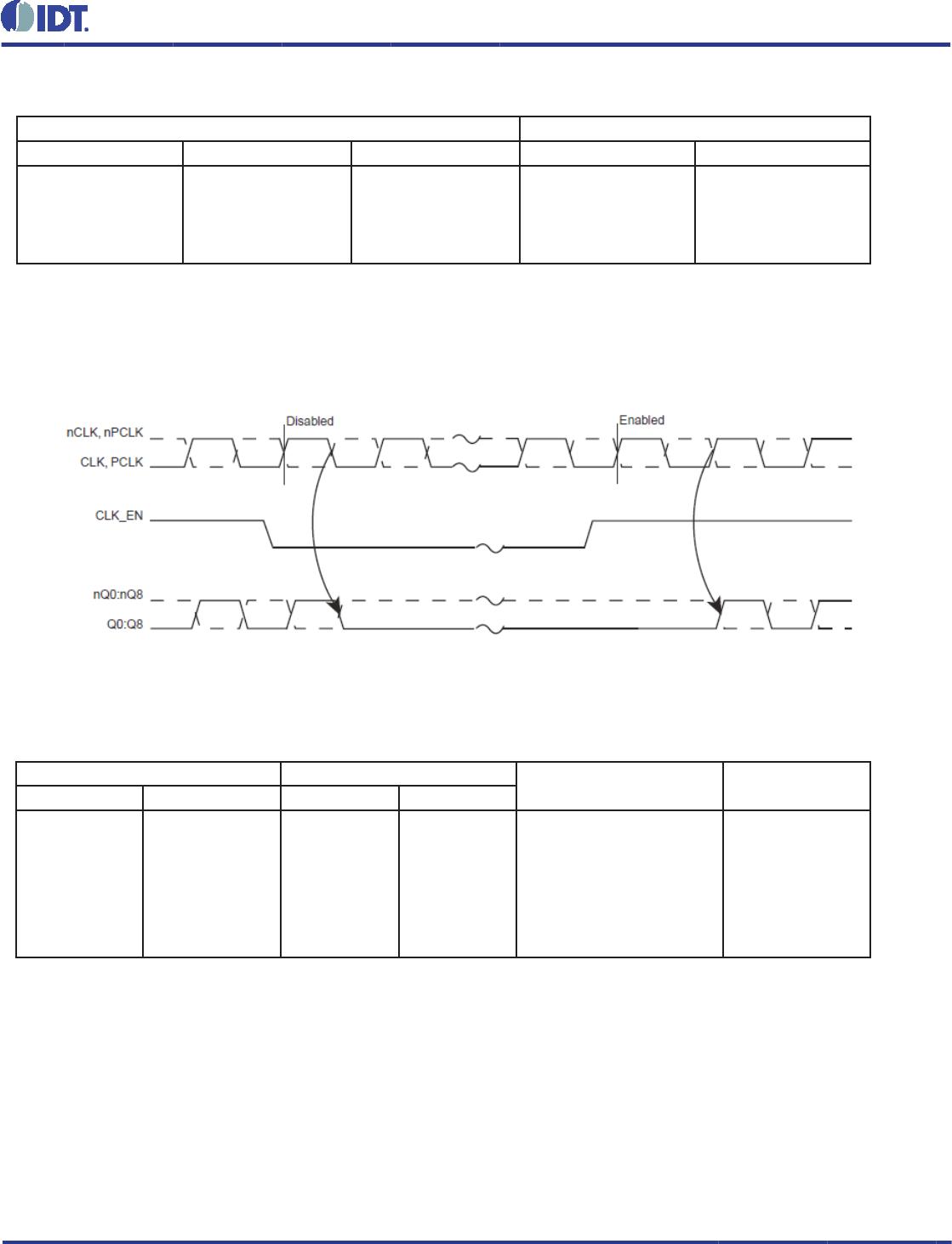
SSTL input levels. The clock enable is internally synchronized
to eliminate runt pulses on the outputs during asynchronous
assertion/deassertion of the clock enable pin.
Guaranteed output skew and part-to-part skew character-
istics make the 8531-01 ideal for high performance work-
station and server applications.
FEATURES
Nine differential 3.3V LVPECL outputs
Selectable differential CLK, nCLK or LVPECL clock inputs
CLK, nCLK pair can accept the following differential
input levels: LVPECL, LVDS, LVHSTL, SSTL, HCSL
PCLK, nPCLK supports the following input types:
LVPECL, CML, SSTL
Maximum output frequency: 500MHz
Translates any single ended input signal (LVCMOS, LVTTL,
GTL) to 3.3V LVPECL levels with resistor bias on nCLK input
Additive phase jitter, RMS: 0.17ps (typical)
Output skew: 50ps (maximum)
Part-to-part skew: 250ps (maximum)
Propagation delay: 2ns (maximum)
3.3V operating supply
0°C to 70°C ambient operating temperature
Available in lead-free (RoHS 6) package
Industrial Temperature information available upon request
BLOCK DIAGRAM PIN ASSIGNMENT
32-Lead LQFP
7mm x 7mm x 1.4mm package body
Y package
Top View
8531-01 Data Sheet
©2016 Integrated Device Technology, Inc Revision F January 19, 20162
TABLE 1. PIN DESCRIPTIONS
TABLE 2. PIN CHARACTERISTICS
Number Name Type Description
1V
CC
Power Power supply pin.
2 CLK Input Pulldown Non-inverting differential clock input.
3 nCLK Input Pullup Inverting differential clock input.
4 CLK_SEL Input Pulldown
Clock Select input. When HIGH, selects PCLK, nPCLK inputs.
When LOW, selects CLK, nCLK. LVTTL / LVCMOS interface levels.
5 PCLK Input Pulldown Non-inverting differential LVPECL clock input.
6 nPCLK Input Pullup Inverting differential LVPECL clock input.
7V
EE
Power Negative supply pin.
8 CLK_EN Input Pullup
Synchronizing clock enable. When HIGH, clock outputs follow clock input.
When LOW, Q outputs are forced low, nQ outputs are forced high.
LVTTL / LVCMOS interface levels.
9, 16, 17,
24, 25, 32
V
CCO
Power Output supply pins.
10, 11 nQ8, Q8 Output Differential output pair. LVPECL interface level.
12, 13 nQ7, Q7 Output Differential output pair. LVPECL interface level.
14, 15 nQ6, Q6 Output Differential output pair. LVPECL interface level.
18, 19 nQ5, Q5 Output Differential output pair. LVPECL interface level.
20, 21 nQ4, Q4 Output Differential output pair. LVPECL interface level.
22, 23 nQ3 Q3 Output Differential output pair. LVPECL interface level.
26, 27 nQ2, Q2 Output Differential output pair. LVPECL interface level.
28, 29 nQ1, Q1 Output Differential output pair. LVPECL interface level.
30, 31 nQ0, Q0 Output Differential output pair. LVPECL interface level.
NOTE: Pullup and Pulldown refer to internal input resistors. See Table 2, Pin Characteristics, for typical values.
Symbol Parameter Test Conditions Minimum Typical Maximum Units
C
IN
Input Capacitance 4 pF
R
PULLUP
Input Pullup Resistor 51
kΩ
R
PULLDOWN
Input Pulldown Resistor 51
kΩ
8531-01 Data Sheet
©2016 Integrated Device Technology, Inc Revision F January 19, 20163
TABLE 3A. CONTROL INPUT FUNCTION TABLE
Inputs Outputs
CLK_EN CLK_SEL Selected Sourced Q0:Q8 nQ0:nQ8
0 0 CLK, nCLK Disabled; LOW Disabled; HIGH
0 1 PCLK, nPCLK Disabled; LOW Disabled; HIGH
1 0 CLK, nCLK Enabled Enabled
1 1 PCLK, nPCLK Enabled Enabled
After CLK_EN switches, the clock outputs are disabled or enabled following a rising and falling input clock edge
as shown in Figure 1.
In the active mode, the state of the outputs are a function of the CLK, nCLK and PCLK, nPCLK inputs as described
in Table 3B.
TABLE 3B. CLOCK INPUT FUNCTION TABLE
Inputs Outputs
Input to Output Mode Polarity
CLK or PCLK nCLK or nPCLK Q0:Q8 nQ0:nQ8
0 1 LOW HIGH Differential to Differential Non Inverting
1 0 HIGH LOW Differential to Differential Non Inverting
0 Biased; NOTE 1 LOW HIGH Single Ended to Differential Non Inverting
1 Biased; NOTE 1 HIGH LOW Single Ended to Differential Non Inverting
Biased; NOTE 1 0 HIGH LOW Single Ended to Differential Inverting
Biased; NOTE 1 1 LOW HIGH Single Ended to Differential Inverting
NOTE 1: Please refer to the Application Information section, “Wiring the Differential Input to Accept Single Ended Levels”.
FIGURE 1. CLK_EN TIMING DIAGRAM

8531AY-01LF

Mfr. #:
Manufacturer:
IDT
Description:
Clock Buffer 1-to-9 LVPECL Fanout Buffer
Lifecycle:
New from this manufacturer.
Delivery:
DHL FedEx Ups TNT EMS
Payment:
T/T Paypal Visa MoneyGram Western Union

Products related to this Datasheet