Nexperia
74AUP1G97
Low-power configurable multiple function gate
74AUP1G97 All information provided in this document is subject to legal disclaimers. © Nexperia B.V. 2017. All rights reserved.
Product data sheet Rev. 10 — 28 March 2017
10 / 25
25 °C -40 °C to +125 °CSymbol Parameter Conditions
Min Typ
[1]
Max Min Max
(85 °C)
Max
(125 °C)
Unit
V
CC
= 2.3 V to 2.7 V 2.4 3.7 5.2 2.1 5.9 6.1 ns
V
CC
= 3.0 V to 3.6 V 2.3 3.4 4.6 1.9 4.9 5.1 ns
C
L
= 15 pF
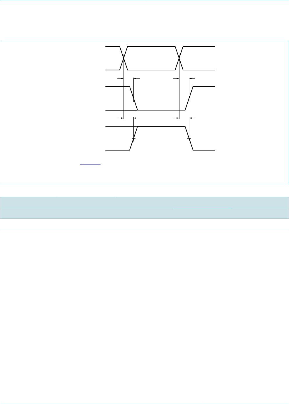
A, B, C to Y; see Figure 15
[2]
V
CC
= 0.8 V - 30.1 - - - - ns
V
CC
= 1.1 V to 1.3 V 3.6 8.2 16.0 3.2 16.7 17.0 ns
V
CC
= 1.4 V to 1.6 V 2.9 5.9 9.6 3.1 10.4 10.9 ns
V
CC
= 1.65 V to 1.95 V 2.8 5.0 7.8 2.5 8.7 9.1 ns
V
CC
= 2.3 V to 2.7 V 2.7 4.2 5.8 2.4 6.5 6.9 ns
t
pd
propagation delay
V
CC
= 3.0 V to 3.6 V 2.5 3.8 5.1 2.2 5.5 5.7 ns
C
L
= 30 pF
A, B, C to Y; see Figure 15
[2]
V
CC
= 0.8 V - 38.3 - - - - ns
V
CC
= 1.1 V to 1.3 V 4.6 10.5 20.9 4.0 21.8 22.2 ns
V
CC
= 1.4 V to 1.6 V 3.7 7.4 12.2 3.8 13.3 14.0 ns
V
CC
= 1.65 V to 1.95 V 3.5 6.3 9.9 3.2 11.1 11.8 ns
V
CC
= 2.3 V to 2.7 V 3.4 5.3 7.4 3.1 8.3 8.8 ns
t
pd
propagation delay
V
CC
= 3.0 V to 3.6 V 3.2 4.9 6.6 2.8 7.0 7.4 ns
C
L
= 5 pF, 10 pF, 15 pF and 30 pF
f
i
= 1 MHz; V
I
= GND to V
CC
[3]
V
CC
= 0.8 V - 2.6 - - - - pF
V
CC
= 1.1 V to 1.3 V - 2.8 - - - - pF
V
CC
= 1.4 V to 1.6 V - 2.9 - - - - pF
V
CC
= 1.65 V to 1.95 V - 3.1 - - - - pF
V
CC
= 2.3 V to 2.7 V - 3.7 - - - - pF
C
PD
power dissipation
capacitance
V
CC
= 3.0 V to 3.6 V - 4.3 - - - - pF
[1] All typical values are measured at nominal V
CC
.
[2] t
pd
is the same as t
PLH
and t
PHL
[3] C
PD
is used to determine the dynamic power dissipation (P
D
in μW).
P
D
= C
PD
x V
CC
2
x f
i
x N + ∑(C
L
x V
CC
2
× f
o
) where:
f
i
= input frequency in MHz;
f
o
= output frequency in MHz;
C
L
= output load capacitance in pF;
V
CC
= supply voltage in V;
N = number of inputs switching;
Σ(C
L
× V
CC
2
× f
o
) = sum of outputs.