10
LTC1563-2/LTC1563-3
156323fa
APPLICATIONS INFORMATION
WUU
U
Functional Description
The LTC1563-2/LTC1563-3 are a family of easy-to-use,
4th order lowpass filters with rail-to-rail operation. The
LTC1563-2, with a single resistor value, gives a unity-gain
filter approximating a Butterworth response. The
LTC1563-3, with a single resistor value, gives a unity-gain
filter approximating a Bessel (linear phase) response. The
proprietary architecture of these parts allows for a simple
unity-gain resistor calculation:
R = 10k(256kHz/f
C
)
where f
C
is the desired cutoff frequency. For many appli-
cations, this formula is all that is needed to design a filter.
For example, a 50kHz filter requires a 51.2k resistor. In
practice, a 51.1k resistor would be used as this is the
closest E96, 1% value available.
The LTC1563-X is constructed with two 2nd order sec-
tions. The output of the first section (section A) is simply
fed into the second section (section B). Note that section
A and section B are similar, but not identical. The parts are
designed to be simple and easy to use.
By simply utilizing different valued resistors, gain, other
transfer functions and higher cutoff frequencies are
achieved. For these applications, the resistor value calcu-
lation gets more difficult. The tables of formulas provided
later in this section make this task much easier. For best
results, design these filters using FilterCAD Version 3.0 (or
newer) or contact the Linear Technology Filter Applica-
tions group for assistance.
Cutoff Frequency (f
C
) and Gain Limitations
The LTC563-X has both a maximum f
C
limit and a mini-
mum f
C
limit. The maximum f
C
limit (256kHz in High Speed
mode and 25.6kHz in the Low Power mode) is set by the
speed of the LTC1563-X’s op amps. At the maximum f
C
,
the gain is also limited to unity.
A minimum f
C
is dictated by the practical limitation of
reliably obtaining large valued, precision resistors. As the
desired f
C
decreases, the resistor value required increases.
When f
C
is 256Hz, the resistors are 10M. Obtaining a
reliable, precise 10M resistance between two points on a
printed circuit board is somewhat difficult. For example, a
10M resistor with only 200M of stray, layout related
resistance in parallel, yields a net effective resistance of
9.52M and an error of –5%. Note that the gain is also
limited to unity at the minimum f
C
.
At intermediate f
C
, the gain is limited by one of the two
reasons discussed above. For best results, design filters
with gain using FilterCAD Version 3 (or newer) or contact
the Linear Technology Filter Applications Group for
assistance.
While the simple formula and the tables in the applications
section deliver good approximations of the transfer func-
tions, a more accurate response is achieved using FilterCAD.
FilterCAD calculates the resistor values using an accurate
and complex algorithm to account for parasitics and op
amp limitations. A design using FilterCAD will always yield
the best possible design. By using the FilterCAD design
tool you can also achieve filters with cutoff frequencies
beyond 256kHz. Cutoff frequencies up to 360kHz are
attainable.
Contact the Linear Technology Filter Applications Group
for a copy the FilterCAD software. FilterCAD can also be
downloaded from our website at www.linear.com.
DC Offset, Noise and Gain Considerations
The LTC1563-X is DC offset trimmed in a 2-step manner.
First, section A is trimmed for minimum DC offset. Next,
section B is trimmed to minimize the total DC offset
(section A
plus
section B). This method is used to give the
minimum DC offset in unity gain applications and most
higher gain applications.
For gains greater than unity, the gain should be distributed
such that most of the gain is taken in section A, with
section B at a lower gain (preferably unity). This type of
gain distribution results in the lowest noise and lowest DC
offset. For high gain, low frequency applications, all of the
gain is taken in section A, with section B set for unity-gain.
In this configuration, the noise and DC offset is dominated
by those of section A. At higher frequencies, the op amps’
finite bandwidth limits the amount of gain that section A
can reliably achieve. The gain is more evenly distributed in
this case. The noise and DC offset of section A is now
multiplied by the gain of section B. The result is slightly
higher noise and offset.
11
LTC1563-2/LTC1563-3
156323fa
APPLICATIONS INFORMATION
WUU
U
Output Loading: Resistive and Capacitive
The op amps of the LTC1563-X have a rail-to-rail output
stage. To obtain maximum performance, the output load-
ing effects must be considered. Output loading issues can
be divided into resistive effects and capacitive effects.
Resistive loading affects the maximum output signal swing
and signal distortion. If the output load is excessive, the
output swing is reduced and distortion is increased. All of
the output voltage swing testing on the LTC1563-X is done
with R22 = 100k and a 10k load resistor. For best undistorted
output swing, the output load resistance should be greater
than 10k.
Capacitive loading on the output reduces the stability of
the op amp. If the capacitive loading is sufficiently high,
the stability margin is decreased to the point of oscillation
at the output. Capacitive loading should be kept below
30pF. Good, tight layout techniques should be maintained
at all times. These parts should not drive long traces and
must never drive a long coaxial cable.
When probing the
LTC1563-X, always use a 10x probe. Never use a 1x probe
.
A standard 10x probe has a capacitance of 10pF to 15pF
while a 1x probe’s capacitance can be as high as 150pF.
The use of a 1x probe will probably cause oscillation.
For larger capacitive loads, a series isolation resistor can
be used between the part and the capacitive load. If the
load is too great, a buffer must be used.
Layout Precautions
The LTC1563-X is an active RC filter. The response of the
filter is determined by the on-chip capacitors and the
external resistors. Any external, stray capacitance in par-
allel with an on-chip capacitor, or to an AC ground, can
alter the transfer function.
Capacitance to an AC ground is the most likely problem.
Capacitance on the LPA or LPB pins does not affect the
transfer function but does affect the stability of the op
amps. Capacitance on the INVA and INVB pins will affect
the transfer function somewhat and will also affect the
stability of the op amps. Capacitance on the SA and SB
pins alters the transfer function of the filter. These pins are
the most sensitive to stray capacitance. Stray capacitance
on these pins results in peaking of the frequency response
near the cutoff frequency. Poor layout can give 0.5dB to
1dB of excess peaking.
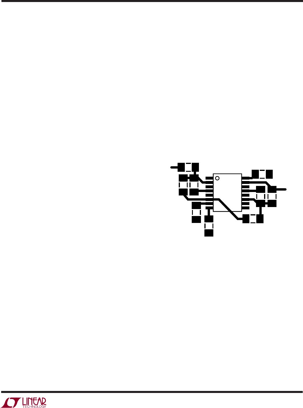
To minimize the effects of parasitic layout capacitance, all
of the resistors for section A should be placed as close as
possible to the SA pin. Place the R31 resistor first so that
it is as close as possible to the SA pin on one end and as
close as possible to the INVA pin on the other end. Use the
same strategy for the layout of section B, keeping all of the
resistors as close as possible to the SB node and first
placing R32 between the SB and INVB pins. It is also best
if the signal routing and resistors are on the same layer as
the part without any vias in the signal path.
Figure 1 illustrates a good layout using the LTC1563-X
with surface mount 0805 size resistors. An even tighter
layout is possible with smaller resistors.
1653 F01
R11
LTC1563-X
R12
R32
R22
R21
R31
V
OUT
V
IN
Figure 1. PC Board Layout
Single Pole Sections and Odd Order Filters
The LTC1563 is configured to naturally form even ordered
filters (2nd, 4th, 6th and 8th). With a little bit of work,
single pole sections and odd order filters are easily achieved.
To form a single pole section you simply use the op amp,
the on-chip C1 capacitor and two external resistors as
shown in Figure 2. This gives an inverting section with the
gain set by the R2-R1 ratio and the pole set by the R2-C1
time constant. You can use this pole with a 2nd order
section to form a noninverting gain 3rd order filter or as a
stand alone inverting gain single pole filter.
Figure 3 illustrates another way of making odd order
filters. The R1 input resistor is split into two parts with an
additional capacitor connected to ground in between the
resistors. This “TEE” network forms a single real pole. RB1
12
LTC1563-2/LTC1563-3
156323fa
should be much larger than RA1 to minimize the interac-
tion of this pole with the 2nd order section. This circuit is
useful in forming dual 3rd order filters and 5th order filters
with a single LTC1563 part. By cascading two parts, 7th
order and 9th order filters are achieved.
DC GAIN = LTC1563-2: C1A = 53.9pF, C1B = 39.2pF
LTC1563-3: C1A = 35pF, C1B = 26.8pF
–R2
R1
F
P
=
1
2π • R2 • C1
1563 F02
+
C1
INV
C2
S
1/2 LTC1563
LP
AGND
R1
(OPEN)
R2
V
OUT
V
IN
Figure 2
RA1
RB1
10
R2RB1RA1 R3
C
P
1563 F03
RA1 • RB1
RA1 + RB1
F
P
=
1
()
2π •C
P
+
C1
INV
C2
S
1/2 LTC1563
LP
AGND
+
(OPEN)
C1
INV
C2
S
1/2 LTC1563
LP
1563 F04
AGND
You can also use the TEE network in both sections of the
part to make a 6th order filter. This 6th order filter does not
conform exactly to the textbook responses. Textbook
responses (Butterworth, Bessel, Chebyshev etc.) all have
three complex pole pairs. This filter has two complex pole
pairs and two real poles. The textbook response always
has one section with a low Q value between 0.5 and 0.6. By
replacing this low Q section with two real poles (two real
poles are the same mathematically as a complex pole pair
with a Q of 0.5) and tweaking the Q of the other two
complex pole pair sections you end up with a filter that is
indistinguishable from the textbook filter. The Typical
Applications section illustrates a 100kHz, 6th order pseudo-
Butterworth filter. FilterCAD is a valuable tool for custom
filter design and tweaking textbook responses.
Figure 3
What To Do with an Unused Section
If the LTC1563 is used as a 2nd or 3rd order filter, one of
the sections is not used. Do not leave this section uncon-
nected. If the section is left unconnected, the output is left
to float and oscillation may occur. The unused section
should be connected as shown in Figure 4 with the INV pin
connected to the LP pin and the S pin left open.
Figure 4
APPLICATIONS INFORMATION
WUU
U

LTC1563-3IGN#PBF

Mfr. #:
Manufacturer:
Analog Devices Inc.
Description:
Active Filter Active RC, 4th Order Lpass Filt Fam
Lifecycle:
New from this manufacturer.
Delivery:
DHL FedEx Ups TNT EMS
Payment:
T/T Paypal Visa MoneyGram Western Union