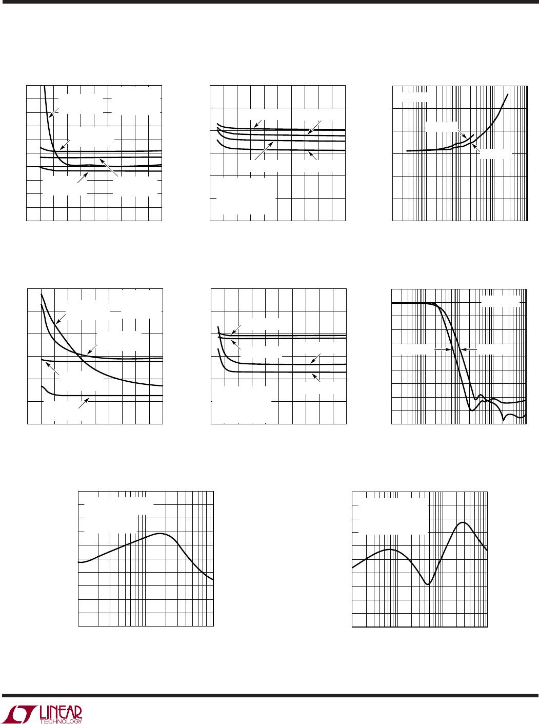
8
LTC1563-2/LTC1563-3
156323fa
LP (Pin 1): Low Power. The LTC1563-X has two operating
modes: Low Power and High Speed. Most applications will
use the High Speed operating mode. Some lower fre-
quency, lower gain applications can take advantage of the
Low Power mode. When placed in the Low Power mode,
the supply current is nearly an order of magnitude lower
than the High Speed mode. Refer to the Applications
Information section for more information on the Low
Power mode.
The LTC1563-X is in the High Speed mode when the
LP input is at a logic high level or is open-circuited. A small
pull-up current source at the LP input defaults the
LTC1563-X to the High Speed mode if the pin is left open.
The part is in the Low Power mode when the pin is pulled
to a logic low level or connected to V
–
.
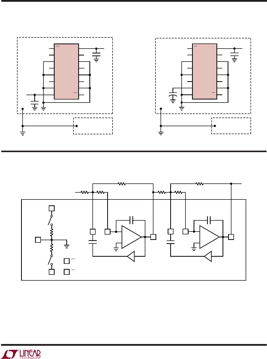
SA, SB (Pins 2, 11): Summing Pins. These pins are a
summing point for signals fed forward and backward.
Capacitance on the SA or SB pin will cause excess peaking
of the frequency response near the cutoff frequency. The
three external resistors for each section should be located
as close as possible to the summing pin to minimize this
effect. Refer to the Applications Information section for
more details.
NC (Pins 3, 5, 10, 12, 14): These pins are not connected
internally. For best performance, they should be con-
nected to ground.
INVA, INVB (Pins 4, 13): Inverting Input. Each of the INV
pins is an inverting input of an op amp. Note that the INV
pins are high impedance, sensitive nodes of the filter and
very susceptible to coupling of unintended signals.
Capacitance on the INV nodes will also affect the fre-
quency response of the filter sections. For these reasons,
printed circuit connections to the INV pins must be kept as
short as possible.
PIN FUNCTIONS
UUU
LPA, LPB (Pins 6, 15): Lowpass Output. These pins are
the rail-to-rail outputs of an op amp. Each output is
designed to drive a nominal net load of 5kΩ and 20pF.
Refer to the Applications Information section for more
details on output loading effects.
AGND (Pin 7): Analog Ground. The AGND pin is the
midpoint of an internal resistive voltage divider developing
a potential halfway between the V
+
and V
–
pins. The
equivalent series resistance is nominally 10kΩ. This serves
as an internal ground reference. Filter performance will
reflect the quality of the analog signal ground. An analog
ground plane surrounding the package is recommended.
The analog ground plane should be connected to any
digital ground at a single point. Figures 1 and 2 show the
proper connections for dual and single supply operation.
V
–
, V
+
(Pins 8, 16): The V
–
and V
+
pins should be
bypassed with 0.1µF capacitors to an adequate analog
ground or ground plane. These capacitors should be
connected as closely as possible to the supply pins. Low
noise linear supplies are recommended. Switching sup-
plies are not recommended as they will decrease the
filter’s dynamic range. Refer to Figures 1 and 2 for the
proper connections for dual and single supply operation.
EN (Pin 9): ENABLE. When the EN input goes high or is
open-circuited, the LTC1563-X enters a shutdown state
and only junction leakage currents flow. The AGND pin, the
LPA output and the LPB output assume high impedance
states. If an input signal is applied to a complete filter
circuit while the LTC1563-X is in shutdown, some signal
will normally flow to the output through passive compo-
nents around the inactive part.
A small internal pull-up current source at the EN input
defaults the LTC1563 to the shutdown state if the EN pin
is left floating
. Therefore, the user
must
connect the EN pin
to V
–
(or a logic low) to enable the part for normal
operation.