3
LT3027
3027fa
PARAMETER CONDITIONS MIN TYP MAX UNITS
GND Pin Current (Per Channel) I
LOAD
= 0mA ● 25 50 µA
V
IN
= V
OUT(NOMINAL)
I
LOAD
= 1mA ● 60 120 µA
(Notes 5, 7) I
LOAD
= 10mA ● 250 400 µA
I
LOAD
= 50mA ● 12 mA
I
LOAD
= 100mA ● 2.4 4 mA
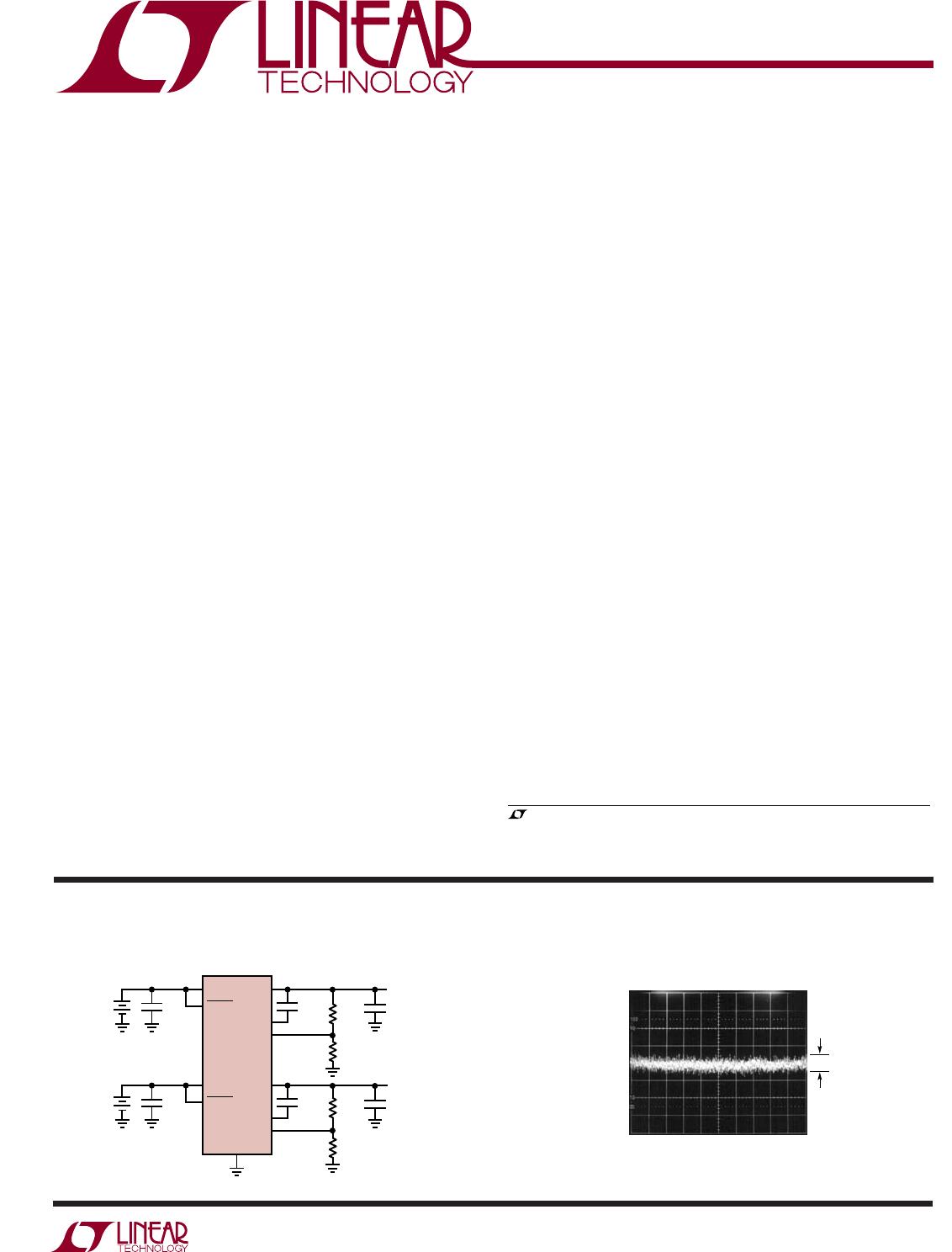
Output Voltage Noise C
OUT
= 10µF, C
BYP
= 0.01µF, I
LOAD
= 100mA, BW = 10Hz to 100kHz 20 µV
RMS
ADJ1/ADJ2 Pin Bias Current (Notes 3, 8) 30 100 nA
Shutdown Threshold V
OUT
= Off to On ● 0.8 1.4 V
V
OUT
= On to Off ● 0.25 0.65 V
SHDN1/SHDN2 Pin Current V
SHDN
= 0V ● 0 0.5 µA
(Note 9) V
SHDN
= 20V ● 13 µA
Quiescent Current in Shutdown V
IN
= 6V, V
SHDN
= 0V (Both SHDN Pins) 0.01 0.1 µA
Ripple Rejection (Note 3) V
IN
= 2.72V (Avg), V
RIPPLE
= 0.5V
P-P
, f
RIPPLE
= 120Hz, 55 65 dB
I
LOAD
= 100mA
Current Limit V
IN
= 7V, V
OUT
= 0V 200 mA
V
IN
= 2.3V, ∆V
OUT
= – 5% ● 110 mA
Input Reverse Leakage Current V
IN
= – 20V, V
OUT
= 0V ● 1mA
The ● denotes specifications which apply over the full operating temperature range, otherwise specifications are T
A
= 25°C. (Note 2)
ELECTRICAL CHARACTERISTICS
Note 5: To satisfy requirements for minimum input voltage, the LT3027 is
tested and specified for these conditions with an external resistor divider
(two 250k resistors) for an output voltage of 2.44V. The external resistor
divider will add a 5µA DC load on the output.
Note 6: Dropout voltage is the minimum input to output voltage differential
needed to maintain regulation at a specified output current. In dropout, the
output voltage will be equal to: V
IN
– V
DROPOUT
.
Note 7: GND pin current is tested with V
IN
= 2.44V and a current source
load. This means the device is tested while operating in its dropout region
or at the minimum input voltage specification. This is the worst-case GND
pin current. The GND pin current will decrease slightly at higher input
voltages.
Note 8: ADJ1 and ADJ2 pin bias current flows into the pin.
Note 9: SHDN1 and SHDN2 pin current flows into the pin.
Note 10: For the LT3027 dropout voltage will be limited by the minimum
input voltage specification under some output voltage/load conditions. See
the curve of Minimum Input Voltage in the Typical Performance
Characteristics.
Note 1: Absolute Maximum Ratings are those values beyond which the life
of a device may be impaired.
Note 2: The LT3027 regulator is tested and specified under pulse load
conditions such that T
J
≈ T
A
. The LT3027E is guaranteed to meet
performance specifications from 0°C to 125°C junction temperature.
Specifications over the –40°C to 125°C operating junction temperature
range are assured by design, characterization and correlation with
statistical process controls. The LT3027I is guaranteed and tested over the
full –40°C to 125°C operating junction temperature range.
Note 3: The LT3027 is tested and specified for these conditions with the
ADJ1/ADJ2 pin connected to the corresponding OUT1/OUT2 pin.
Note 4: Operating conditions are limited by maximum junction
temperature. The regulated output voltage specification will not apply for
all possible combinations of input voltage and output current. When
operating at maximum input voltage, the output current range must be
limited. When operating at maximum output current, the input voltage
range must be limited.