9
LT3027
3027fa
APPLICATIO S I FOR ATIO
WUUU
The LT3027 is a dual 100mA low dropout regulator with
independent inputs, micropower quiescent current and
shutdown. The device is capable of supplying 100mA per
channel at a dropout voltage of 300mV. Output voltage
noise can be lowered to 20µV
RMS
over a 10Hz to 100kHz
bandwidth with the addition of a 0.01µF reference bypass
capacitor. Additionally, the reference bypass capacitor will
improve transient response of the regulator, lowering the
settling time for transient load conditions. The low oper-
ating quiescent current (25µA per channel) drops to less
than 1µA in shutdown. In addition to the low quiescent
current, the LT3027 regulator incorporates several pro-
tection features which make it ideal for use in battery-
powered systems. The device is protected against reverse
input voltages. Additionally, in dual supply applications
where the regulator load is returned to a negative supply,
the output can be pulled below ground by as much as 20V
and still allow the device to start and operate.
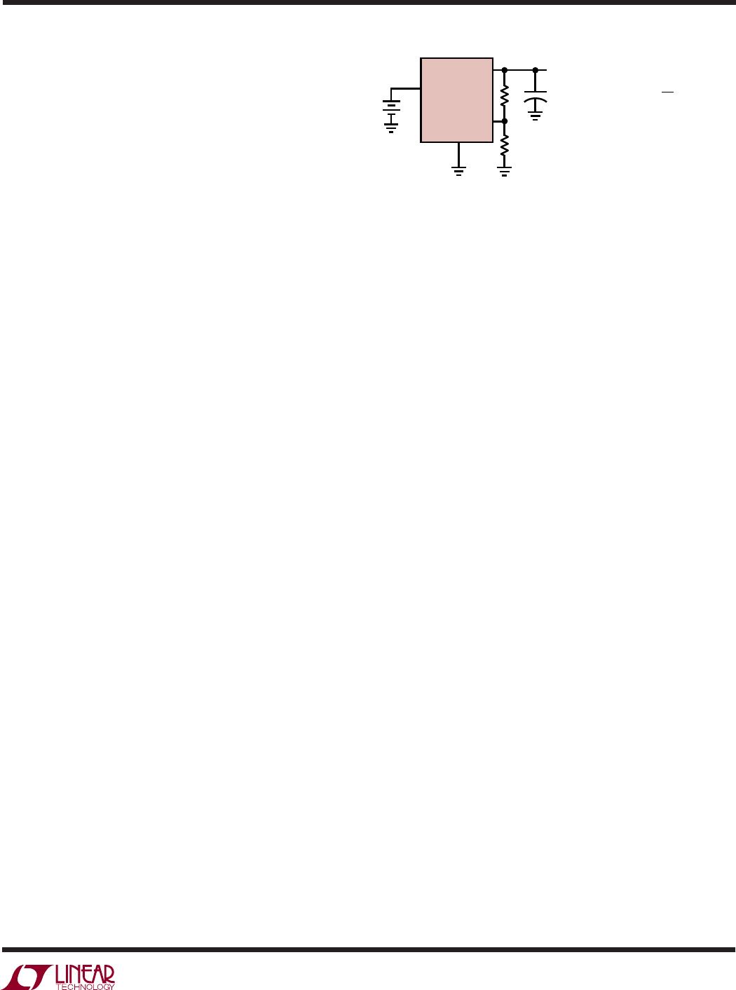
Adjustable Operation
The LT3027 has an output voltage range of 1.22V to 20V.
The output voltage is set by the ratio of two external resis-
tors as shown in Figure 1. The device servos the output to
maintain the corresponding ADJ pin voltage at 1.22V ref-
erenced to ground. The current in R1 is then equal to 1.22V/
R1 and the current in R2 is the current in R1 plus the ADJ
pin bias current. The ADJ pin bias current, 30nA at 25°C,
flows through R2 into the ADJ pin. The output voltage can
be calculated using the formula in Figure 1. The value of R1
should be no greater than 250k to minimize errors in the
output voltage caused by the ADJ pin bias current. Note that
in shutdown the output is turned off and the divider current
will be zero. Curves of ADJ Pin Voltage vs Temperature and
ADJ Pin Bias Current vs Temperature appear in the Typical
Performance Characteristics.
The device is tested and specified with the ADJ pin tied to
the corresponding OUT pin for an output voltage of 1.22V.
Specifications for output voltages greater than 1.22V will
be proportional to the ratio of the desired output voltage to
1.22V: V
OUT
/1.22V. For example, load regulation for an
output current change of 1mA to 100mA is –1mV typical
at V
OUT
= 1.22V. At V
OUT
= 12V, load regulation is:
(12V/1.22V)(–1mV) = –9.8mV
Bypass Capacitance and Low Noise Performance
The LT3027 regulator may be used with the addition of a
bypass capacitor from V
OUT
to the corresponding BYP pin
to lower output voltage noise. A good quality low leakage
capacitor is recommended. This capacitor will bypass the
reference of the regulator, providing a low frequency noise
pole. The noise pole provided by this bypass capacitor will
lower the output voltage noise to as low as 20µV
RMS
with
the addition of a 0.01µF bypass capacitor. Using a bypass
capacitor has the added benefit of improving transient
response. With no bypass capacitor and a 10µF output
capacitor, a 10mA to 100mA load step will settle to within
1% of its final value in less than 100µs. With the addition
of a 0.01µF bypass capacitor, the output will stay within
1% for a 10mA to 100mA load step (see Transient Reponse
in Typical Performance Characteristics section). However,
regulator start-up time is inversely proportional to the size
of the bypass capacitor, slowing to 15ms with a 0.01µF
bypass capacitor and 10µF output capacitor.
Figure 1. Adjustable Operation
IN
3027 F01
R2
LT3027
OUT
V
IN
V
OUT
ADJ
GND
R1
+
VV
R
R
IR
VV
InAATC
OUTPUT RANGE V TO V
OUT ADJ
ADJ
ADJ
=+
⎛
⎝
⎜
⎞
⎠
⎟
+
()()
=
=°
122 1
2
1
2
122
30 25
122 20
.
.
= .

